Photonic metamaterial
| Electromagnetism |
|---|
 |
|
|
A photonic metamaterial (PM), also known as an optical metamaterial, is a type of electromagnetic metamaterial, that interacts with light, covering terahertz (THz), infrared (IR) or visible wavelengths.[1] The materials employ a periodic, cellular structure.
The subwavelength periodicity distinguishes photonic metamaterials from photonic band gap or photonic crystal structures. The cells are on a scale that is magnitudes larger than the atom, yet much smaller than the radiated wavelength,[2][3] are on the order of nanometers.[2][3][4]
In a conventional material, the response to electric and magnetic fields, and hence to light, is determined by atoms.[5][6] In metamaterials, cells take the role of atoms in a material that is homogeneous at scales larger than the cells, yielding an effective medium model.[2][3][5]
Some photonic metamaterials exhibit magnetism at high frequencies, resulting in strong magnetic coupling. This can produce a negative index of refraction in the optical range.
Potential applications include cloaking and transformation optics.[7]
Photonic crystals differ from PM in that the size and periodicity of their scattering elements are larger, on the order of the wavelength. Also, a photonic crystal is not homogeneous, so it is not possible to define values of ε (permittivity) or u (permeability).[8]
History
While researching whether or not matter interacts with the magnetic component of light, Victor Veselago (1967) envisioned the possibility of refraction with a negative sign, according to Maxwell's equations. A refractive index with a negative sign is the result of permittivity, ε < 0 (less than zero) and magnetic permeability, μ < 0 (less than zero).[4][9] Veselago's analysis has been cited in over 1500 peer reviewed articles and many books.[10][11][12][13]

In the mid-1990s, metamaterials were first seen as potential technologies for applications such as nanometer-scale imaging and cloaking objects. As of 2015, metamaterial antennas were commercially available.[14]
Negative permeability was achieved with a split-ring resonator (SRR) as part of the subwavelength cell. The SRR achieved negative permeability within a narrow frequency range. This was combined with a symmetrically positioned electric conducting post, which created the first negative index metamaterial, operating in the microwave band. Experiments and simulations demonstrated the presence of a left-handed propagation band, a left-handed material. The first experimental confirmation of negative index of refraction occurred soon after, also at microwave frequencies.[4][15][16]
Negative permeability and negative permittivity

Natural materials, such as precious metals, can achieve ε < 0 up to the visible frequencies. However, at terahertz, infrared and visible frequencies, natural materials have a very weak magnetic coupling component, or permeability. In other words, susceptibility to the magnetic component of radiated light can be considered negligible.[9]
Negative index metamaterials behave contrary to the conventional "right-handed" interaction of light found in conventional optical materials. Hence, these are dubbed left-handed materials or negative index materials (NIMs), among other nomenclatures.[4][15][16]
Only fabricated NIMs exhibit this capability. Photonic crystals, like many other known systems, can exhibit unusual propagation behavior such as reversal of phase and group velocities. However, negative refraction does not occur in these systems.[15][17][18]
Naturally occurring ferromagnetic and antiferromagnetic materials can achieve magnetic resonance, but with significant losses. In natural materials such as natural magnets and ferrites, resonance for the electric (coupling) response and magnetic (coupling) response do not occur at the same frequency.
Optical frequency
Photonic metamaterial SRRs have reached scales below 100 nanometers, using electron beam and nanolithography. One nanoscale SRR cell has three small metallic rods that are physically connected. This is configured as a U shape and functions as a nano-inductor. The gap between the tips of the U-shape function as a nano-capacitor. Hence, it is an optical nano-LC resonator. These "inclusions" create local electric and magnetic fields when externally excited. These inclusions are usually ten times smaller than the vacuum wavelength of the light c0 at the resonance frequency. The inclusions can then be evaluated by using an effective medium approximation.[4][10]
PMs display a magnetic response with useful magnitude at optical frequencies. This includes negative permeability, despite the absence of magnetic materials. Analogous to ordinary optical material, PMs can be treated as an effective medium that is characterized by effective medium parameters ε(ω) and μ(ω), or similarly, εeff and μeff.[10][19]
Effective medium model
An effective (transmission) medium approximation describes material slabs that, when reacting to an external excitation, are "effectively" homogeneous, with corresponding "effective" parameters that include "effective" ε and µ and apply to the slab as a whole. Individual inclusions or cells may have values different from the slab.[20][21]
Coupling magnetism
Negative magnetic permeability was originally achieved in a left-handed medium at microwave frequencies by using arrays of split-ring resonators.[22] In most natural materials, the magnetically coupled response starts to taper off at frequencies in the gigahertz range, which implies that significant magnetism does not occur at optical frequencies. The effective permeability of such materials is unity, μeff = 1. Hence, the magnetic component of a radiated electromagnetic field has virtually no effect on natural occurring materials at optical frequencies.[23]
In metamaterials the cell acts as a meta-atom, a larger scale magnetic dipole, analogous to the picometer-sized atom. For meta-atoms constructed from gold, μ < 0 can be achieved at telecommunication frequencies but not at visible frequencies. The visible frequency has been elusive because the plasma frequency of metals is the ultimate limiting condition.[6]
Design and fabrication
Optical wavelengths are much shorter than microwaves, making subwavelength optical metamaterials more difficult to realize. Microwave metamaterials can be fabricated from circuit board materials, while lithography techniques must be employed to produce PMs.
Successful experiments used a periodic arrangement of short wires or metallic pieces with varied shapes. In a different study the whole slab was electrically connected.
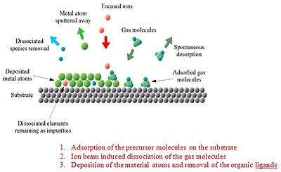
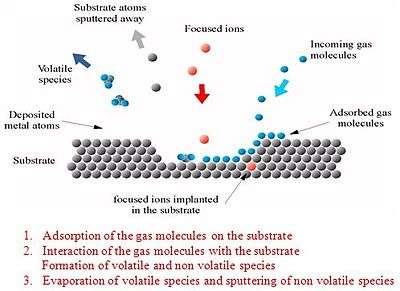
Fabrication techniques include electron beam lithography, nanostructuring with a focused ion beam and interference lithography.[10][24][25][26]
In 2014 a polarization-insensitive metamaterial prototype was demonstrated to absorb energy over a broad band (a super-octave) of infrared wavelengths. The material displayed greater than 98% measured average absorptivity that it maintained over a wide ±45° field-of-view for mid-infrared wavelengths between 1.77 and 4.81 μm. One use is to conceal objects from infrared sensors. Palladium provided greater bandwidth than silver or gold. A genetic algorithm randomly modified an initial candidate pattern, testing and eliminating all but the best. The process was repeated over multiple generations until the design became effective.[27][28]
The metamaterial is made of four layers on a silicon substrate. The first layer is palladium, covered by polyimide (plastic) and a palladium screen on top. The screen has sub-wavelength cutouts that block the various wavelengths. A polyimide layer caps the whole absorber. It can absorb 90 percent of infrared radiation at up to a 55 degree angle to the screen. The layers do not need accurate alignment. The polyimide cap protects the screen and helps reduce any impedance mismatch that might occur when the wave crosses from the air into the device.[28]
Research
One-way transmission
In 2015 visible light joined microwave and infrared NIMs in propagating light in only one direction. ("mirrors" instead reduce light transmission in the reverse direction, requiring low light levels behind the mirror to work.)[29]
The material combined two optical nanostructures: a multi-layered block of alternating silver and glass sheets and metal grates. The silver-glass structure is a "hyperbolic" metamaterial, which treats light differently depending on which direction the waves are traveling. Each layer is tens of nanometers thick—much thinner than visible light's 400 to 700 nm wavelengths, making the block opaque to visible light, although light entering at certain angles can propagate inside the material.[29]
Adding chromium grates with sub-wavelength spacings bent incoming red or green light waves enough that they could enter and propagate inside the block. On the opposite side of the block, another set of grates allowed light to exit, angled away from its original direction. The spacing of the exit grates was different from that of the entrance grates, bending incident light so that external light could not enter the block from that side. Around 30 times more light passed through in the forward direction than in reverse. The intervening blocks reduced the need for precise alignment of the two grates with respect to each other.[29]
Such structures hold potential for applications in optical communication—for instance, they could be integrated into photonic computer chips that split or combine signals carried by light waves. Other potential applications include biosensing using nanoscale particles to deflect light to angles steep enough to travel through the hyperbolic material and out the other side.[29]
Lumped circuit elements
By employing a combination of plasmonic and non-plasmonic nanoparticles, lumped circuit element nanocircuits at infrared and optical frequencies appear to be possible. Conventional lumped circuit elements are not available in a conventional way.[30]
Subwavelength lumped circuit elements proved workable in the microwave and radio frequency (RF) domain. The lumped element concept allowed for element simplification and circuit modularization. Nanoscale fabrication techniques exist to accomplish subwavelength geometries.[30]
Cell design
Metals such as gold, silver, aluminum and copper conduct currents at RF and microwave frequencies. At optical frequencies characteristics of some noble metals are altered. Rather than normal current flow, plasmonic resonances occur as the real part of the complex permittivity becomes negative. Therefore, the main current flow is actually the electric displacement current density ∂D / ∂t, and can be termed as the “flowing optical current".[30]
At subwavelength scales the cell's impedance becomes dependent on shape, size, material and the optical frequency illumination. The particle's orientation with the optical electric field may also help determine the impedance. Conventional silicon dielectrics have the real permittivity component εreal > 0 at optical frequencies, causing the nanoparticle to act as a capacitive impedance, a nanocapacitor. Conversely, if the material is a noble metal such as gold or silver, with εreal < 0, then it takes on inductive characteristics, becoming a nanoinductor. Material loss is represented as a nano-resistor.[30][31]
Tunability
The most commonly applied scheme to achieve a tunable index of refraction is electro-optical tuning. Here the change in refractive index is proportional to either the applied electric field, or is proportional to the square modulus of the electric field. These are the Pockels effect and Kerr effects, respectively.
An alternative is to employ a nonlinear optical material and depend on the optical field intensity to modify the refractive index or magnetic parameters.[32]
Layering
Stacking layers produces NIMs at optical frequencies. However, the surface configuration (non-planar, bulk) of the SRR normally prevents stacking. Although a single-layer SRR structure can be constructed on a dielectric surface, it is relatively difficult to stack these bulk structures due to alignment tolerance requirements.[4] A stacking technique for SRRs was published in 2007 that uses dielectric spacers to apply a planarization procedure to flatten the SRR layer.[33] It appears that arbitrary many layers can be made this way, including any chosen number of unit cells and variant spatial arrangements of individual layers.[4][33][34]
Frequency doubling
In 2014 researchers announced a 400 nanometer thick frequency-doubling non-linear mirror that can be tuned to work at near-infrared to mid-infrared to terahertz frequencies. The material operates with much lower intensity light than traditional approaches. For a given input light intensity and structure thickness, the metamaterial produced approximately one million times higher intensity output. The mirrors do not require matching the phase velocities of the input and output waves.[35]
It can produce giant nonlinear response for multiple nonlinear optical processes, such as second harmonic, sum- and difference-frequency generation, as well a variety of four-wave mixing processes. The demonstration device converted light with a wavelength of 8000 to 4000 nanometers.[35]
The device is made of a stack of thin layers of indium, gallium and arsenic or aluminum, indium and arsenic. 100 of these layers, each between one and twelve nanometers thick, were faced on top by a pattern of asymmetrical, crossed gold nanostructures that form coupled quantum wells and a layer of gold on the bottom.[35]
Potential applications include remote sensing and medical applications that call for compact laser systems.[35]
Other
Dyakonov surface waves[36] (DSW) relate to birefringence related to photonic crystals, metamaterial anisotropy.[37] Recently photonic metamaterial operated at 780 nanometer (near-infrared),[38][39][40] 813 nm and 772 nm.[41][42]
See also
- Terahertz gap
- Negative index metamaterials
- History of metamaterials
- Metamaterial cloaking
- Photonic metamaterials
- Metamaterial
- Metamaterial antennas
- Nonlinear metamaterials
- Photonic crystal
- Seismic metamaterials
- Split-ring resonator
- Acoustic metamaterials
- Metamaterial absorber
- Plasmonic metamaterials
- Terahertz metamaterials
- Tunable metamaterials
- Transformation optics
- Theories of cloaking
- Metamaterials (journal)
- Metamaterials Handbook
- Metamaterials: Physics and Engineering Explorations
General references
- Shalaev, Vladimir M., et al. Negative Index of Refraction in Optical Metamaterials arXiv.org. 17 pages.
- Shalaev, Vladimir M., et al. Negative index of refraction in optical metamaterials Opt. Lett. Vol. 30. 2005-12-30. 3 pages
References
- ↑ K.V.Sreekanth; Zeng, Shuwen; Shang, Jingzhi; Yong, Ken-Tye; Yu, Ting (2012). "Excitation of surface electromagnetic waves in a graphene-based Bragg grating". Scientific Reports. 2. Bibcode:2012NatSR...2E.737S. doi:10.1038/srep00737. PMC 3471096
 . PMID 23071901.
 - 1 2 3 "Photonic Metamaterials". Encyclopedia of Laser Physics and Technology. I & II. Wiley. p. 1. Retrieved 2009-10-01.
- 1 2 3 Capolino, Filippo (October 2009). Applications of Metamaterials. Taylor & Francis. pp. 29–1, 25–14, 22–1. ISBN 978-1-4200-5423-1. Retrieved 2009-10-01.
- 1 2 3 4 5 6 7 Ozbay, Ekmel (2008-11-01). "The Magical World of Photonic Metamaterials" (PDF). Optics and Photonics News. 19 (11): 22–27. doi:10.1364/OPN.19.11.000022. Archived from the original (Free PDF download) on July 19, 2011. Retrieved 2009-12-07.
- 1 2 Pendry, John (2006). "Photonics: Metamaterials in the sunshine" (PDF). Nature Materials. 5 (8): 599–600. Bibcode:2006NatMa...5..599P. doi:10.1038/nmat1697. PMID 16880801. Retrieved 2009-10-08.
- 1 2 Linden, Stefan; Enkrich, Christian; Dolling, Gunnar; Klein, Matthias W.; Zhou, Jiangfeng; Koschny, Thomas; Soukoulis, Costas M.; Burger, Sven; Schmidt, Frank; Wegener, Martin (2006). "Photonic Metamaterials: Magnetism at Optical Frequencies" (PDF). IEEE Journal of selected topics in quantum electronics. 12 (6): 1097. doi:10.1109/JSTQE.2006.880600.
- ↑ Vladimir M., Shalaev. "Metamaterials: A New Paradigm of Physics and Engineering". Optical Metamaterials Fundamentals and Applications by Wenshan Cai and Vladimir Shalaev. Springer (book publisher) (Book publication date: November 30, 2009. ISBN 978-1-4419-1150-6. Archived from the original (Lecture date (Part 1): March 06, 2008) on August 21, 2009. Retrieved 2010-02-06. External link in
|title=(help) - ↑ Smith, David; Pendry, John B.; Wiltshire, M. C. K. (2004-08-06). "Metamaterials and Negative Refractive Index" (PDF). Science. 305 (5685): 788–792. Bibcode:2004Sci...305..788S. doi:10.1126/science.1096796. PMID 15297655. Archived from the original (see page 791. Free PDF download. PDF supplies links to other related articles, on this topic. This article cited by 452.) on June 13, 2010. Retrieved 2010-01-13.
- 1 2 Shalaev, Vladimir M (January 2007). "Optical negative-index metamaterials" (PDF). Nature photonics. 1 (1): 41. Bibcode:2007NaPho...1...41S. doi:10.1038/nphoton.2006.49. Retrieved 2009-11-20.
- 1 2 3 4 Capolino, Filippo (October 2009). Applications of Metamaterials (Chapter title: - "Fabrication and Optical Characterization of Photonic Metamaterials"). Taylor & Francis. pp. 29–1, chapter 29. ISBN 978-1-4200-5423-1.access date:2009-12-31
- ↑ Pendry, John B.; Smith, David R. (June 2004). "Reversing Light: Negative Refraction" (Free PDF download. Cited by 185. Alternate copy here.). Physics Today. 57 (6): 37–44. Bibcode:2004PhT....57f..37P. doi:10.1063/1.1784272. Retrieved 2009-11-30.
- ↑ Crossref.org forward linking technology (December 2009). "Article citing "The Electrodynamics of Substances with Simultaneously Negative values of ε and μ" (The number of articles citing this work according to Cross ref.org). by Victor G. Veselago. Retrieved 2009-12-06.
- ↑ Engheta, Nader and; Richard W. Ziolkowski (April 2005). "A Positive Future for Double-Negative Metamaterials" (Free PDF download. Cited by 165 papers.). IEEE Transactions on Microwave Theory and Techniques. 53 (4): 1535. Bibcode:2005ITMTT..53.1535E. doi:10.1109/TMTT.2005.845188. Retrieved 2010-02-15.
- ↑ "Kymeta technology". Retrieved April 2015. Check date values in:
|access-date=(help) - 1 2 3 Pendry, J., "New electromagnetic materials emphasize the negative," Physics World, 1–5, 2001
- 1 2 "Negative confirmation" (this is an online magazine format and free access is available.). Nature, Physics portal. Nature Publishing Group. 2003. p. 01. Retrieved 2010-03-15.
- ↑ Smith, David R.; Kroll, Norman (2000-10-02). "Negative Refractive Index in Left-Handed Materials" (PDF). Physical Review Letters. 85 (14): 2933–2936. Bibcode:2000PhRvL..85.2933S. doi:10.1103/PhysRevLett.85.2933. PMID 11005971. Archived from the original (PDF) on July 19, 2011. Retrieved 2010-01-04.
- ↑ Srivastava, R.; et al. (2008). "Negative refraction by Photonic Crystal" (PDF). Progress in Electromagnetics Research B (PIER B). 2: 15–26. doi:10.2528/PIERB08042302. Archived from the original (Free PDF download) on July 19, 2010. Retrieved 2010-01-04.
- ↑ Boltasseva, Alexandra and; Vladimir M. Shalaev (2008-03-18). "Fabrication of optical negative-index metamaterials: Recent advances and outlook" (Free PDF download.). Metamaterials. Elsevier B.V. 2: 1–17. Bibcode:2008MetaM...2....1B. doi:10.1016/j.metmat.2008.03.004. Retrieved 2010-01-29.
- ↑ Shadrivov, Ilya V.; Kozyrev, AB; Van Der Weide, DW; Kivshar, YS (2008-11-24). "Nonlinear magnetic metamaterials" (Introduction section. Free PDF download). Optics Express. 16 (25): 20266–71. Bibcode:2008OExpr..1620266S. doi:10.1364/OE.16.020266. PMID 19065165. Retrieved 2009-11-26.
- ↑ Caloz, Christophe; Itoh, Tatsuo (November 2005). Electromagnetic metamaterials: transmission line theory and microwave applications (Free online download of limited preview.). Wiley, John & Sons, Incorporated. p. 11. ISBN 0-471-66985-7. Retrieved 2009-11-15.
- ↑ Shelby, R. A.; Smith, DR; Schultz, S (2001). "Experimental Verification of a Negative Index of Refraction". Science. 292 (5514): 77–9. Bibcode:2001Sci...292...77S. doi:10.1126/science.1058847. PMID 11292865.
- ↑ Grigorenko AN, et al. (2005-11-17). "Nanofabricated media with negative permeability at visible frequencies". Nature (Free PDF download.). 438 (7066): 335–338. arXiv:physics/0504178. Bibcode:2005Natur.438..335G. doi:10.1038/nature04242. PMID 16292306.
- ↑ Orloff, J.; Utlaut, M.; Swanson, L. (2003). High Resolution Focused Ion Beams: FIB and Its Applications. Springer Press. ISBN 0-306-47350-X.
- ↑ Lucille A. Giannuzzi, North Carolina State University (18 May 2006). Introduction to Focused Ion Beams: Instrumentation, Theory, Techniques and Practice. Springer Science & Business Media. ISBN 978-0-387-23313-0.
- ↑ Kochz, J.; Grun, K.; Ruff, M.; Wernhardt, R.; Wieck, A.D. (1999). Creation of nanoelectronic devices by focused ion beam implantation.
- ↑ Jeremy A. Bossard; et al. (2014). "Near-Ideal Optical Metamaterial Absorbers with Super-Octave Bandwidth". ACS Nano. doi:10.1021/nn4057148.
- 1 2 "Genetic algorithm used to design broadband metamaterial". KurzweilAI. May 7, 2014. Check date values in:
|access-date=(help); - 1 2 3 4 "New NIST metamaterial gives light a one-way ticket". R&D. 2014-07-02. Check date values in:
|access-date=(help); - 1 2 3 4 Engheta, Nader (2007-09-21). "Circuits with Light at Nanoscales: Optical Nanocircuits Inspired by Metamaterials" (PDF). Science. 317 (5845): 1698–1702. Bibcode:2007Sci...317.1698E. doi:10.1126/science.1133268. PMID 17885123. Retrieved 2010-01-18.
- ↑ Engheta, Nader; Alessandro Salandrino, and Andrea Al�uz (2005-08-26). "Circuit Elements at Optical Frequencies: Nanoinductors, Nanocapacitors, and Nanoresistor". Physical Review Letters. 95 (9): 095504 (4 pages). arXiv:cond-mat/0411463. Bibcode:2005PhRvL..95i5504E. doi:10.1103/PhysRevLett.95.095504. Retrieved 2010-01-29. Cite uses deprecated parameter
|coauthors=(help); replacement character in|coauthors=at position 37 (help) - ↑ Wang, Xiande; et al. (2007-10-04). "Tunable optical negative-index metamaterials employing anisotropic liquid crystals" (Free PDF download.). Applied Physics Letters. 91 (14): 143122. Bibcode:2007ApPhL..91n3122W. doi:10.1063/1.2795345. Retrieved 2009-10-02.
- 1 2 Liu, Na; Guo, Hongcang; Fu, Liwei; Kaiser, Stefan; Schweizer, Heinz; Giessen, Harald (2007-12-02). "Three-dimensional photonic metamaterials at optical frequencies" (PDF). Nature Materials. 7 (1): 31–37. Bibcode:2008NatMa...7...31L. doi:10.1038/nmat2072. PMID 18059275. Retrieved 2009-10-07.
- ↑ Valentine, Jason; et al. (2008-08-11). "Three-dimensional optical metamaterial with a negative refractive index" (PDF). Nature. 455 (7211): 376–379. Bibcode:2008Natur.455..376V. doi:10.1038/nature07247. PMID 18690249. Retrieved 2009-09-28.
- 1 2 3 4 "New nonlinear metamaterial is a million times better than traditional options". R&D. 2014-07-02. Retrieved April 2015. Check date values in:
|access-date=(help) - ↑ Dyakonov, M. I. (April 1988). "New type of electromagnetic wave propagating at an interface". Soviet Physics JETP. 67 (4): 714.
- ↑ Artigas, David and; Torner, Lluis (2005-01-03). "Dyakonov Surface Waves in Photonic Metamaterials" (PDF). Phys. Rev. Lett. 94 (1): 013901. Bibcode:2005PhRvL..94a3901A. doi:10.1103/PhysRevLett.94.013901. PMID 15698082. Retrieved 2009-10-08.
- ↑ Zhang, Shuang; et al. (2005-09-23). "Experimental Demonstration of Near-Infrared Negative-Index Metamaterials" (PDF). Phys. Rev. Lett. 95 (13): 137404. arXiv:physics/0504208. Bibcode:2005PhRvL..95m7404Z. doi:10.1103/PhysRevLett.95.137404. PMID 16197179. Archived from the original (PDF) on July 26, 2008. Retrieved 2009-10-05.
- ↑ Dolling, G.; Wegener, M.; Soukoulis, C.M.; Linden, S. (2006-12-13). "Negative-index metamaterial at 780 nm wavelength". Optics Letters. 32 (1): 53–55. arXiv:physics/0607135. Bibcode:2007OptL...32...53D. doi:10.1364/OL.32.000053. PMID 17167581.
- ↑ Shalaev, Vladimir M. (January 2007). "Optical negative-index metamaterials" (free PDF article is linked to this reference). Nature photonics. 1 (1): 41–48. Bibcode:2007NaPho...1...41S. doi:10.1038/nphoton.2006.49.
- ↑ Chettiar, U. K.; Kildishev, AV; Yuan, HK; Cai, W; Xiao, S; Drachev, VP; Shalaev, VM (2007-06-05). "Dual-Band Negative Index Metamaterial: Double-Negative at 813 nm and Single-Negative at 772 nm". Optics Letters (Free PDF download). 32 (12): 1671–1673. arXiv:physics/0612247. Bibcode:2007OptL...32.1671C. doi:10.1364/OL.32.001671. PMID 17572742.
- ↑ Caloz, Christophe; Gupta, Shulabh (2008-03-28). "Phase-engineered Metamaterial Structures and Devices". Progress in Electromagnetics Research Symposium (Session 2A3 Metamaterials at Optical Frequencies): 10. Archived from the original (The 23rd PIERS 2008 in Hangzhou, CHINA. Free PDF download is also available.) on 2010-07-05. Retrieved 2009-11-15.
- Litchinitser, N.M.; V.M. Shalaev (2008-02-03). "Photonic metamaterials" (PDF). Laser Phys. Lett. 5 (6): 411–420 (2008). Bibcode:2008LaPhL...5..411L. doi:10.1002/lapl.200810015.
External links
- Optics and photonics: Physics enhancing our lives
- OPAL: A Computational Tool For Photonics
- Experimental Verification of Reversed Cherenkov Radiation...
- Oriented Assembly of Metamaterials Particle self-assembly suggested for assembly of metamaterials at optical wavelengths.
- Subpicosecond Optical Switching with a Negative Index Metamaterial