Phosphorene

Phosphorene is a two-dimensional material and allotrope of phosphorus. Phosphorene can be viewed as a single layer of black phosphorus, much in the same way that graphene is a single layer of graphite. Phosphorene is predicted to be a strong competitor to graphene because, in contrast to graphene, phosphorene has a band gap.[1][2] Phosphorene was first isolated in 2014 by mechanical exfoliation.[3][4][5]
History
Elemental phosphorus was discovered in 1669 by Hennig Brand. In the 1960s black phosphorus, a layered semiconducting allotrope of phosphorus, was synthesized, which exhibited high carrier mobility.[6] In 2014, several groups [3][4][5] introduced single-layer phosphorene, a monolayer of black phosphorus. It attracted renewed attention[7] because of its potential in optoelectronics and electronics due to its band gap, which can be tuned via modifying its thickness, anisotropic photoelectronic properties and high carrier mobility.[5][8][9][10][11][12][13][14] Phosphorene was initially prepared using mechanical cleavage, a commonly used technique in graphene production that is difficult to scale up. Liquid exfoliation[15][16] is a promising method for scalable phosphorene production.

Synthesis

Synthesis of phosphorene is a significant challenge. Currently, there are two main ways of phosphorene production: scotch-tape-based microcleavage[5] and liquid exfoliation,[15][16] while several other methods are being developed as well. Phosphorene production from plasma etching is also reported.[18]
In scotch-tape-based microcleavage,[5] phosphorene is mechanically exfoliated from a bulk of black phosphorus crystal using scotch-tape. Phosphorene is then transferred on a Si/SiO2 substrate, where it is then cleaned with acetone, isopropyl alcohol and methanol to remove any scotch tape residue. The sample is then heated to 180 °C to remove solvent residue.
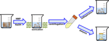
In the liquid exfoliation method first reported by Brent et al. in 2014[19] and modified by others,[15] bulk black phosphorus is first ground in a mortar and pestle and then sonicated in deoxygenated, anhydrous organic liquids such as NMP under inert atmosphere using low-power bath sonication. Suspensions are then centrifuged for 30 minutes to filter out the unexfoliated black phosphorus. Resulting 2D monolayer and few-layer phosphorene unoxidized and crystalline structure, while exposure to air oxidizes the phosphorene and produces acid.[15]
Another variation of liquid exfoliation[16] is “basic N-methyl-2-pyrrolidone (NMP) liquid exfoliation”. Bulk black phosphorene is added to a saturated NaOH/NMP solution, which is further sonicated for 4 hours to conduct liquid exfoliation. The solution is then centrifuged twice, first for 10 minutes to remove any unexfoliated black phosphorus and then for 20 minutes at higher speed to separate thick layers of phosphorene (5–12 layers) from NMP. The supernatant then is centrifuged again at higher speed for another 20 minutes to separate thinner layers of phosphorene (1–7 layers). The precipitate from centrifugation is then redispersed in water and washed several times by deionized water. Phosphorene/water solution is dropped onto silicon with a 280-nm SiO2 surface, where it is further dried under vacuum. NMP liquid exfoliation method was shown to yield phosphorene with controllable size and layer number, excellent water stability and in high yield.[16]
However, the high yield production of phosphorene has been demonstrated by many groups in solvents, but to realize the potential applications of this material, it is crucial to deposit these free-standing nanosheets in solvents systematically on substrates. Recently, H. Kaur et. al.[20] demonstrated the synthesis, interface driven alignment and subsequent functional properties of few layer semiconducting phosphorene using Langmuir-Blodgett assembly. This is the first study which provides a straightforward and versatile solution towards the challenge of assembling nanosheets of phosphorene onto various supports and subsequently use these sheets in an electronic device. Therefore wet assemblies techniques like Langmuir-Blodgett serves as a very valuable new entry point for the exploration of electronic as well as opto-electronic properties of phosphorene as well as other 2D layered inorganic materials.
It is still a challenge to directly epitaxially grow 2D phosphorene because the stability of black phosphorene is highly sensitive to substrate, which is understanding by theoretical simulations.[21][22]
Properties
Structure
Phosphorene 2D materials are composed of individual layers held together by van der Waals forces in lieu of covalent or ionic bonds that are found in most materials. There are five electrons on 3p orbitals of phosphorus atom, thus, giving rise to sp3 hybridization of phosphorus atom within phosphorene structure. Monolayered phosphorene exhibits the structure of a quadrangular pyramid because three electrons of P atom bond with three other P atoms covalently at 2.18 A° leaving one lone pair.[15] Two of the phosphorus atoms are in the plane of the layer at 99° from one another, and the third phosphorus is between the layers at 103°, yielding an average angle of 102°.
According to density functional theory (DFT) calculations, phosphorene forms in a honeycomb lattice structure with notable nonplanarity in the shape of structural ridges. It is predicted that crystal structure of black phosphorus can be discriminated under high pressure.[23] This is mostly due to the anisotropic compressibility of black phosphorus because of the asymmetrical crystal structures. Subsequently, the van der Waals bond can be greatly compressed in the z-direction. However, there is a great variation in compressibility across the orthogonal x-y plane.
It is reported that controlling the centrifugal speed of production may aid in regulating the thickness of a material. For example, centrifuging at 18000 rpm during synthesis produced phosphorene with an average diameter of 210 nm and a thickness of 2.8 ± 1.5 nm (2–7 layers).[15]
Band gap and conductivity properties

Phosphorene has a thickness dependent direct band gap that changes to 1.88 eV in a monolayer from 0.3 eV in the bulk.[16] Increase in band gap value in single-layer phosphorene is predicted to be caused by the absence of interlayer hybridization near the top of the valence and bottom of the conduction band.[5] A pronounced peak centered at around 1.45 eV suggests the band gap structure in few- or single-layer phosphorene difference from bulk crystals.[5]
In vacuum or on weak substrate, a interesting reconstruction with nanotubed termination of phosphorene edge is very easy to happen, transforming phosphorene edge from metallic to semiconducting.[24]
Air stability

One major disadvantage of phosphorene is its air-stability.[26][27][28][29][30][31] Composed of hygroscopic phosphorus and with extremely high surface-to-volume ratio, phosphorene reacts with water vapor and oxygen assisted by visible light[32] to degrade within the scope of hours. Through the degradation process, phosphorene (solid) reacts with oxygen/water to develop liquid phase acid 'bubbles' on the surface, and finally evaporate (vapor) to fully vanish (S-B-V degradation) and severely reducing overall quality.[16]
Applications
Transistor
Researchers[5] have fabricated transistors of phosphorene to examine its performance in actual devices. Phosphorene-based transistor consists of a channel of 1.0 μm and uses few layered phosphorene with a thickness varying from 2.1 to over 20 nm. Reduction of the total resistance with decreasing gate voltage is observed, indicating the p-type characteristic of phosphorene. Linear I-V relationship of transistor at low drain bias suggests good contact properties at the phosphorene/metal interface. Good current saturation at high drain bias values was observed.[5] However, it was seen that the mobility is reduced in few-layer phosphorene when compared to bulk black phosphorus. Field-effect mobility of phosphorene-based transistor shows a strong thickness dependence, peaking at around 5 nm and decrease steadily with further increase of crystal thickness.
Atomic layer deposition (ALD) dielectric layer and/or hydrophobic polymer is used as encapsulation layers in order to prevent device degradation and failure. Phosphorene devices are reported to maintain their function for weeks with encapsulation layer, whereas experience device failure within a week when exposed to ambient condition.[26][27][28][29][30]
Inverter
Researchers have also constructed the CMOS inverter (logic circuit) by combining a phosphorene PMOS transistor with a MoS2 NMOS transistor, achieving high heterogeneous integration of semiconducting phosphorene crystals as a new channel material for potential electronic applications.[5] In the inverter, the power supply voltage is set to be 1 V. The output voltage shows a clear transition from VDD to 0 within the input voltage range from −10 to −2 V. A maximum gain of ~1.4 is attained.
Solar-cell donor material (optoelectronics)
The potential applications of mixed bilayer phosphorene in solar-cell material was examined as well.[33] The predicted power conversion efficiency for a monolayer MoS2/AA-stacked bilayer phosphorene and MoS2/AB-stacked bilayer phosphorene can get as high as ~18% and 16%, respectively. Results suggest that trilayer MoS2 phosphorene is a promising candidate in flexible optoelectronic devices.[33]
Flexible circuits

Phosphorene is a promising candidate for flexible nano systems due to its ultra-thin nature with ideal electrostatic control and superior mechanical flexibility.[36] Researchers have demonstrated the flexible transistors, circuits and AM demodulator based on few-layer phosphorus, showing enhanced am bipolar transport with high room temperature carrier mobility as high as ~310 cm2/Vs and strong current saturation. Fundamental circuit units including digital inverter, voltage amplifier and frequency doubler have been realized.[34] Radio frequency (RF) transistors with highest intrinsic cutoff frequency of 20 GHz has been realized for potential applications in high frequency flexible smart nano systems.[35]
See also
References
| Wikimedia Commons has media related to Phosphorene. |
- ↑ Roberts, Kristin (28 July 2015). "Five reasons phosphorene may be a new wonder material – MagLab". nationalmaglab.org.
- ↑ Carvalho, Alexandra; Wang, Min; Zhu, Xi; Rodin, Aleksandr S.; Su, Haibin; Castro Neto, Antonio H. (2016). "Phosphorene: from theory to applications". Nature Review Materials. doi:10.1038/natrevmats.2016.61.
- 1 2 Li, Likai; Yu, Yijun; Jun Ye, Guo; Ge, Qingqin; Ou, Xuedong; Wu, Hua; Zhang, Yuanbo (2014). "Black Phosphorus Field Effect Transistors". Nature Nanotechnology. 9: 372–377. doi:10.1038/nnano.2014.35.
- 1 2 Koenig, Steven P.; Doganov, Rostislav A.; Schmidt, Henrrik; Castro Neto, Antonio H.; Ozyilmaz, Barbaros (2014). "Electric Field Effect in Ultrathin Black Phosphorus". Applied Physics Letters. 104: 103106. doi:10.1063/1.4868132.
- 1 2 3 4 5 6 7 8 9 10 Liu, Han; Neal, Adam T.; Zhu, Zhen; Luo, Zhe; Xu, Xianfan; Tománek, David; Ye, Peide D. (2014). "Phosphorene: An Unexplored 2D Semiconductor with a High Hole Mobility". ACS Nano. 8 (4): 4033–4041. doi:10.1021/nn501226z. PMID 24655084.
- ↑ Warschauer, Douglas (1963). "Electrical and Optical Properties of Crystalline Black Phosphorus". Journal of Applied Physics. 34 (7): 1853–1860. doi:10.1063/1.1729699.
- ↑ Castellanos-Gomez, Andres; Vicarelli, Leonardo; Prada, Elsa; Island, Joshua O; Narasimha-Acharya, K L; Blanter, Sofya I; Groenendijk, Dirk J; Buscema, Michele; Steele, Gary A (2014). "Isolation and characterization of few-layer black phosphorus". 2D Materials. 1 (2): 025001. doi:10.1088/2053-1583/1/2/025001.
- ↑ Xia, Fengnian; Wang, Han; Jia, Yichen (2014). "Rediscovering black phosphorus as an anisotropic layered material for optoelectronics and electronics". Nature Communications. 5. doi:10.1038/ncomms5458.
- ↑ Churchill, Hugh O. H.; Jarillo-Herrero, Pablo (2014). "Two-dimensional crystals: Phosphorus joins the family". Nature Nanotechnology. 9 (5): 330–331. doi:10.1038/nnano.2014.85. PMID 24801536.
- ↑ Koenig, Steven P.; Doganov, Rostislav A.; Schmidt, Hennrik; Neto, A. H. Castro; Özyilmaz, Barbaros (2014). "Electric field effect in ultrathin black phosphorus". Applied Physics Letters. 104 (10): 103106. doi:10.1063/1.4868132.
- ↑ Rodin, A. S.; Carvalho, A.; Castro Neto, A. H. (2014). "Strain-Induced Gap Modification in Black Phosphorus". Physical Review Letters. 112 (17): 176801. doi:10.1103/PhysRevLett.112.176801. PMID 24836264.
- ↑ Buscema, Michele; Groenendijk, Dirk J.; Blanter, Sofya I.; Steele, Gary A.; van der Zant, Herre S. J.; Castellanos-Gomez, Andres (2014). "Fast and Broadband Photoresponse of Few-Layer Black Phosphorus Field-Effect Transistors". Nano Letters. 14 (6): 3347–3352. doi:10.1021/nl5008085. PMID 24821381.
- ↑ Qiao, Jingsi; Kong, Xianghua; Hu, Zhi-Xin; Yang, Feng; Ji, Wei (2014). "High-mobility transport anisotropy and linear dichroism in few-layer black phosphorus". Nature Communications. 5: 4475. doi:10.1038/ncomms5475. PMC 4109013
 . PMID 25042376.
 - ↑ Li, Likai; Yu, Yijun; Ye, Guo Jun; Ge, Qingqin; Ou, Xuedong; Wu, Hua; Feng, Donglai; Chen, Xian Hui; Zhang, Yuanbo (2014). "Black phosphorus field-effect transistors". Nature Nanotechnology. 9 (5): 372–377. doi:10.1038/nnano.2014.35. PMID 24584274.
- 1 2 3 4 5 6 Woomer, Adam H.; Farnsworth, Tyler W.; Hu, Jun; Wells, Rebekah A.; Donley, Carrie L.; Warren, Scott C. (2015). "Phosphorene: Synthesis, Scale-Up, and Quantitative Optical Spectroscopy". ACS Nano. 9 (9): 8869–8884. doi:10.1021/acsnano.5b02599. PMID 26256770.
- 1 2 3 4 5 6 Guo, Zhinan; Zhang, Han; Lu, Shunbin; Wang, Zhiteng; Tang, Siying; Shao, Jundong; Sun, Zhengbo; Xie, Hanhan; Wang, Huaiyu (2015). "From Black Phosphorus to Phosphorene: Basic Solvent Exfoliation, Evolution of Raman Scattering, and Applications to Ultrafast Photonics". Advanced Functional Materials. 25: n/a. doi:10.1002/adfm.201502902.
- ↑ Ezawa, M. (2014). "Topological origin of quasi-flat edge band in phosphorene". New Journal of Physics. 16 (11): 115004. doi:10.1088/1367-2630/16/11/115004.
- ↑ Reich, Eugenie Samuel (4 February 2014). "Phosphorene excites materials scientists". Nature News & Comment.
- 1 2 Brent, J. R.; Savjani, N.; Lewis, E. A.; Haigh, S. J.; Lewis, D. J.; O'Brien, P. (2014). "Production of few-layer phosphorene by liquid exfoliation of black phosphorus". Chem. Commun. 50 (87): 13338–13341. doi:10.1039/C4CC05752J.
- ↑ Ritu, Harneet (2016). "Large Area Fabrication of Semiconducting Phosphorene by Langmuir-Blodgett Assembly". Sci. Rep. 6: 34095. doi:10.1038/srep34095.
- ↑ Gao, Junfeng (2016). "The Critical Role of Substrate in Stabilizing Phosphorene Nanoflake: A Theoretical Exploration". J. Am. Chem. Soc. 138 (14): 4763–4771. doi:10.1021/jacs.5b12472.
- ↑ "Understanding how flat phosphorus grows". Phys.Org. 9 Sep 2014.
- ↑ Jamieson, John C. (1963-03-29). "Crystal Structures Adopted by Black Phosphorus at High Pressures". Science. 139 (3561): 1291–1292. doi:10.1126/science.139.3561.1291. PMID 17757066.
- ↑ Gao, Junfeng (2016). "Nanotube-Terminated Zigzag Edge of Phosphorene formed by Self-Rolling Reconstruction". Nanoscale. doi:10.1039/C6NR06201F.
- ↑ Kim, Joon-Seok; Liu, Yingnan; Zhu, Weinan; Kim, Seohee; Wu, Di; Tao, Li; Dodabalapur, Ananth; Lai, Keji; Akinwande, Deji (2015-03-11). "Toward air-stable multilayer phosphorene thin-films and transistors". Scientific Reports. 5: 8989. doi:10.1038/srep08989. PMC 4355728. PMID 25758437.
- 1 2 Kim, Joon-Seok; Liu, Yingnan; Zhu, Weinan; Kim, Seohee; Wu, Di; Tao, Li; Dodabalapur, Ananth; Lai, Keji; Akinwande, Deji (11 March 2015). "Toward air-stable multilayer phosphorene thin-films and transistors". Scientific Reports. 5: 8989. doi:10.1038/srep08989. PMC 4355728. PMID 25758437.
- 1 2 Luo, Xi; Rahbarihagh, Yaghoob; Hwang, James C. M.; Liu, Han; Du, Yuchen; Ye, Peide D. (December 2014). "Temporal and Thermal Stability of Al2O3-Passivated Phosphorene MOSFETs". IEEE Electron Device Letters. 35 (12): 1314–1316. doi:10.1109/LED.2014.2362841.
- 1 2 Wood, Joshua D.; Wells, Spencer A.; Jariwala, Deep; Chen, Kan-Sheng; Cho, EunKyung; Sangwan, Vinod K.; Liu, Xiaolong; Lauhon, Lincoln J.; Marks, Tobin J.; Hersam, Mark C. (10 December 2014). "Effective Passivation of Exfoliated Black Phosphorus Transistors against Ambient Degradation". Nano Letters. 14 (12): 6964–6970. arXiv:1411.2055. doi:10.1021/nl5032293. PMID 25380142.
- 1 2 Koenig, Steven P.; Doganov, Rostislav A.; Schmidt, Hennrik; Castro Neto, A. H.; Özyilmaz, Barbaros (10 March 2014). "Electric field effect in ultrathin black phosphorus". Applied Physics Letters. 104 (10): 103106. doi:10.1063/1.4868132.
- 1 2 Island, Joshua O; Steele, Gary A; Zant, Herre S J van der; Castellanos-Gomez, Andres (13 January 2015). "Environmental instability of few-layer black phosphorus". 2D Materials. 2 (1): 011002. doi:10.1088/2053-1583/2/1/011002.
- ↑ Castellanos-Gomez, Andres; Vicarelli, Leonardo; Prada, Elsa; Island, Joshua O; Narasimha-Acharya, K L; Blanter, Sofya I; Groenendijk, Dirk J; Buscema, Michele; Steele, Gary A; Alvarez, J V; Zandbergen, Henny W; Palacios, J J; van der Zant, Herre S J (25 June 2014). "Isolation and characterization of few-layer black phosphorus". 2D Materials. 1 (2): 025001. doi:10.1088/2053-1583/1/2/025001.
- ↑ Favron, Alexandre; et al. "Exfoliating pristine black phosphorus down to the monolayer: photo-oxidation and quantum confinement". arXiv. Cornell University. arXiv:1408.0345v2.
- 1 2 Dai, Jun; Zeng, Xiao Cheng (2014). "Bilayer Phosphorene: Effect of Stacking Order on Bandgap and Its Potential Applications in Thin-Film Solar Cells". The Journal of Physical Chemistry Letters. 5 (7): 1289–1293. doi:10.1021/jz500409m. PMID 26274486.
- 1 2 Zhu, Weinan; Yogeesh, Maruthi N.; Yang, Shixuan; Aldave, Sandra H.; Kim, Joon-Seok; Sonde, Sushant; Tao, Li; Lu, Nanshu; Akinwande, Deji (2015-03-11). "Flexible Black Phosphorus Ambipolar Transistors, Circuits and AM Demodulator". Nano Letters. 15 (3): 1883–1890. doi:10.1021/nl5047329. ISSN 1530-6984. PMID 25715122.
- 1 2 Zhu, Weinan; Park, Saungeun; Yogeesh, Maruthi N.; McNicholas, Kyle M.; Bank, Seth R.; Akinwande, Deji (2016-04-13). "Black Phosphorus Flexible Thin Film Transistors at Gighertz Frequencies". Nano Letters. 16 (4): 2301–2306. doi:10.1021/acs.nanolett.5b04768. ISSN 1530-6984.
- ↑ Akinwande, Deji; Petrone, Nicholas; Hone, James (2014). "Two-dimensional flexible nanoelectronics". Nature Communications. 5: 5678. doi:10.1038/ncomms6678. PMID 25517105.