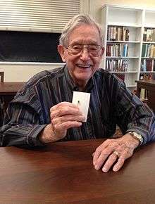
James R. Biard
| James R. Biard | |
|---|---|
 US Inventor of the GaAs Infrared LED | |
| Born |
May 20, 1931 Paris, Texas |
| Residence | United States |
| Nationality | American |
| Fields | Electrical engineering |
| Alma mater | Texas A&M University; BS 1954, MS 1956, PhD 1957 |
Dr. James R. "Bob" Biard (born May 20, 1931) is an American electrical engineer and inventor who holds 73 U.S. patents including the first commercial light-emitting diode (LED),[1] the optical isolator,[2] the Schottky transistor,[3] and Metal Oxide Semiconductor Read Only Memory (MOS ROM).[4] He has been on the staff of Texas A&M University as an Adjunct Professor of Electrical Engineering since 1980.
The GaAs IR Light-Emitting Diode
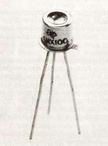
In September 1961, while working at Texas Instruments Inc. in Dallas, TX, Dr. Biard and Gary E. Pittman discovered infrared light emission from a forward biased tunnel diode constructed on gallium arsenide (GaAs) semi-insulating substrate. On August 8, 1962, Biard and Pittman filed a patent based on their findings, which described a zinc diffused p-n junction LED with spaced cathode contacts to allow for efficient emission of infrared light under forward bias. After establishing the priority of their work based on engineering notebooks predating submissions from G.E. Labs, RCA Research Labs, IBM Research Labs, Bell Labs, and Lincoln Labs at MIT, the U.S. patent office issued the two inventors U.S. patent 3,293,513 for the GaAs infrared (IR) light-emitting diode, the first practical LED.[5] After filing the patent, T.I. immediately began a project to manufacture infrared diodes. They announced the first commercial LED product (the SNX-100) in October 1962. T.I. gave Biard and Pittman $1.00 each for their patent.
Infrared LEDs continue to be used today as transmitters in fiber optic data communication systems. They are also used in the remote control units of many commercial products including televisions, DVD players, and other domestic appliances.
Life and career
Bob grew up and attended school in Paris, TX where his father, James Christopher "Jimmy" Biard of Biardstown, worked as a farmer and a Dr. Pepper route salesman for the local Dr. Pepper company. His father eventually became manager of the local 7-Up company and ended up buying it from the former owner. His father also sold used cars, worked as a master plumber at Camp Maxey (an army camp north of Paris) during and after WW-II, and did plumbing work for homes and businesses in the Paris area. Later in life Jimmy became chief deputy sheriff in Lamar County, TX. Bob’s mother, Mary Ruth Biard (née Bills), worked as a retail sales person at the Collegiate Shop in downtown Paris. She also sang in quartets at weddings and funerals. For the first six years of Bob's life, the only thing he was able to eat was mashed overripe bananas, stewed apples, and homemade dried cottage cheese. Since his father was a Dr. Pepper salesman, he knew all of the local grocery store owners. They would save the overripe bananas for Bob. His mother made the cottage cheese by placing unpasteurized milk in a cup towel and hanging it on an outdoor clothes line. While in high school, Bob worked for his father and an off duty fireman, who was also a plumber, during the summer as a plumber's assistant.
After receiving an associate degree from Paris Junior College in 1951, Bob transferred to Texas A&M University in College Station, TX where he received a B.S. in Electrical Engineering (June 1954), an M.S. in Electrical Engineering (January 1956), and a Ph.D. in Electrical Engineering (May 1957). Among the scholarships Biard received were the Dow-Corning Award in 1953-54, and the Westinghouse and Texas Power & Light fellowships throughout his graduate work. He was also a member of IRE, Eta Kappa Nu, Tau Beta Pi, Phi Kappa Phi, and an associate member of Sigma Xi. In 1956 he worked part-time for the Texas Engineering Experiment Station supervising operation and maintenance of EESEAC, the Station's analog computer. During grad school he also designed several vacuum tube DC amplifiers. His PhD dissertation was entitled, "Further Investigation of Electronic Multiplication of Voltages By Use of Logarithms". While a student at Texas A&M, he met his wife Amelia Ruth Clark. They married on May 23, 1952 and later moved to Richardson, TX. Together they have 3 children (Jimmy, Jan, and Becky), 10 grandchildren, and 8 great-grandchildren.

On June 3, 1957, three days after graduation, Dr. Biard was hired, along with his former Texas A&M professor Walter T. Matzen, by Texas Instruments Inc. in Dallas, TX. Here his work focused on the development of transistor circuits, microwave and optoelectronic components, avalanche photodiodes, silicon MOS Technology, high frequency transmission lines, solid state devices, and compound semiconductor materials technology. In the summer of 1958, Texas Instruments hired Jack Kilby (the inventor of the integrated circuit). According to Dr. Biard, during TI’s annual two-week summer shutdown, "At the time we were new, so we had to work while the others were on vacation. He would often come by and talk to us." Kilby held more than 60 U.S. patents, including two with Dr. Biard (the first optical isolator - US3304431 and an electro-optical transistor switching device - US3413480). Biard later stated, "I had the pleasure of being the co-inventor on two of his 60 patents. It was an honor to have my name with his."

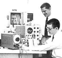
In 1959, Dr. Biard and Gary Pittman were assigned to work together in the Semiconductor Research and Development Laboratory (SRDL) at Texas Instruments on the creation of GaAs varactor diodes used in X-band radar receivers. While investigating the valley current region of a tunnel diode they had constructed on a zinc diffused area of gallium arsenide semi-insulating substrate, they discovered a significant drop in resistance between the two Ohmic side contacts, when the diode was operated in forward bias. This photoconductive response in the semi-insulating substrate material was a result of photon emission, however, the photons were infrared, which cannot be seen by the human eye. In September 1961, using an infrared image converter microscope recently brought in from Japan, they discovered all of the GaAs varactor diodes and tunnel diodes they had manufactured at the time emitted infrared light. By October they demonstrated efficient light emission and signal coupling between a GaAs p-n junction light emitter and an electrically isolated semiconductor photodetector. On August 8, 1962, Biard and Pittman filed a patent based on their findings titled "Semiconductor Radiant Diode". After four years spent establishing the priority of their work, the U.S. patent office issued the two inventors the patent for the GaAs infrared (IR) light-emitting diode. Most other organized research seeking LEDs at the time used II-VI semiconductors like cadmium sulfide (CdS) and cadmium telluride (CdTe), while Biard and Pittman's patent used gallium arsenide (GaAs), a III/V semiconductor. Based on their findings, T.I. immediately began a project to manufacture infrared diodes. In October 1962, they announced the first commercial LED product (the SNX-100), which sold for a price of $130 per unit. The SNX-100 employed a pure GaAs crystal to emit a 900 nm light output. It used gold-zinc for the P-type contact and tin alloy for the N-type contact. An IBM Card Verifier was the first commercial device to use infrared LEDs. The LEDs replaced tungsten bulbs that controlled punched card readers. Infrared light was sent through the holes or blocked by the card, which not only significantly reduced the size and power required, but also improved the reliability. In November 1978, Tom M. Hyltin, a former engineering manager at Texas Instruments, published a book titled "The Digital Electronic Watch", in which he cited Dr. Biard and Gary Pittman's 1961 discovery as being fundamentally important to the creation of the digital wrist-watch.
In August 2013, during a recollection of the patent, Dr. Biard stated the following:
The first diodes that we saw emitting light were not designed to be LEDs. They were varactor diodes and tunnel diodes, which had all of the N-type surface and P-type surface covered with Ohmic contact to achieve a low series resistance. At the time, the varactor diodes had an etched mesa geometry and the IR light came out around the edge of the mesa. On the tunnel diodes, the light could be seen at the edges of the chip. They did not emit very much light, but it was enough for us to see with the IR image converter microscope. That led us to create a structure in which the N-type surface of the chip had spaced contacts, so the light emitted at the junction could be emitted from most of the top surface of the chip. Gary made those spaced N-type Ohmic contacts by tin plating metal wires and alloying the tin on the surface of the wire to the N-type GaAs surface. With a rectangular chip of GaAs, most of the light emitted at the junction was reflected at the exit surface. The index of refraction of GaAs is 3.6 and air has an index of 1.0. This means that ~97% of the light emitted at the junction is totally internally reflected at the exit surface. The highest quantum efficiency that can be expected from a rectangular LED chip is ~2%, even with an anti-reflection coating on the optical exit surface. This total internal reflection problem led us to come up with the hemispherical dome LED. In this diode the N-type GaAs substrate is shaped into a hemisphere and the hemispherical surface is covered with an anti-reflection coating (preferably silicon nitride) to minimize front surface reflection. The LED P-N junction is in the center of the flat face of the hemisphere. The central P-type region is covered with the anode Ohmic contact. The cathode Ohmic contact was a donut shape that covered most of the remainder of the N-type flat surface of the hemisphere. By making the diameter of the hemisphere 3.6 times larger than the diameter of the P-type layer, all the light at the exit surface of the hemisphere was inside the critical angle for total internal reflection. This resulted in a huge increase in quantum efficiency because up to 50% of the light emitted at the junction could escape from the chip at the hemispherical exit surface. The other half of the light went toward the P-type Ohmic contact and was absorbed in the GaAs. The absorption in the thicker N-type GaAs between the junction and exit surface resulted in less improvement in quantum efficiency than what we had hoped for, however, the dome LEDs were much more efficient.
On November 29, 1963 Dr. Biard, Gary Pittman, Edward L. Bonin, and Jack Kilby filed a patent titled "Photosensitive Transistor Chopper Using Light Emissive Diode" (U.S. Patent US3304431); the first optical isolator. Within the patent they described a phototransistor chopper consisting of an LED optically coupled with a dual emitter, photosensitive, silicon transistor. The arrangement provided a switching function in which the switch was completely electrically isolated from the LED that drove it. The transistor operated in response to light emitted from the LED when forward current bias was generated across the junction of the diode. When emitted light struck the surface of the transistor, it was absorbed in the regions of both the emitter-base and base-collector junctions causing the transistor to conduct. This photoconductive transistor could be rapidly turned on and off by intensity modulating the LED at a very high frequency using high frequency alternating voltage. Prior to their invention, complete electrical isolation of the switch element in a chopper from the driving source for opening and closing the switch element was not possible, even through use of isolation transformers. Using isolation transformers, which were bulky and expensive, in miniaturized circuits to separate the driving source and the switch element resulted in magnetic pick-up and spike feed-through due to the transformer winding capacitance. Optical isolators were ideal because they're very small and can be mounted to a circuit board. In addition, they offer protection against excessively high voltages, reduce noise levels, and make measurements more accurate. In March 1965, Texas Instruments announced the SNX1304 Optoelectronic Pulse Amplifier, which was conceived and developed by Dr. Biard and Jerry Merryman, the inventor of the first handheld digital calculator. The SNX1304 consisted of a GaAs p-n junction light emitter optically coupled to an integrated silicon photodetector feedback-amplifier circuit. The device is thought to be the first commercial optically coupled integrated circuit.
In the mid-1960s, Dr. Biard was placed in charge of both the Optoelectronic branch and the MOS branch in the Semiconductor Research and Development Lab (SRDL) at Texas Instruments. In 1964, TI's Opto branch developed a monolithic visible LED element consisting of a 3x5 array of red LEDs capable of displaying the numbers 0-9. The device was lacking a means of driving the array, so Dr. Biard and Bob Crawford (from the MOS branch) designed a P-channel MOS circuit using binary coded decimal inputs to turn on the appropriate 15 output lines. The MOS circuit worked on the first pass and was implemented into a simulated cockpit altimeter. In March of that year, TI displayed the altimeter in a booth at the New York IEEE show and convention. At this convention, TI also demonstrated a hearing aid, which was the first consumer product using TI's integrated circuit. Biard and Crawford filed a patent for their device (U.S. Patent US3541543) on July 25, 1966, referred to as the "Binary Decoder". This was the first time a Read Only Memory had been made using MOS transistors. In the 1980s, while employed for Honeywell, Dr. Biard testified before the International Trade Commission in Washington D.C., per the request of Texas Instruments, in a royalties suit regarding Japanese firms using their Binary Decoder patent in their own MOS ROM circuits. The judge in the lawsuit determined that the Japanese firms did not violate TI's patent rights because they had made enough changes in the implementation of their circuits. By the late 1970s, MOS ROM devices had become the most common example of nonvolatile memory used to provide the storage of fixed programs in digital equipment such as calculators and microprocessor systems.
In 1964, Dr. Biard designed linear transimpedance amplifiers (TIA) to work with silicon photodiodes for receiving optical signals generated by LEDs. When the signal current from the silicon photodiode was too large, the input stage of the amplifier would saturate and cause undesirable delays when the optical signal was removed. Dr. Biard solved this problem by connecting a silicon HP Schottky diode across the collector-base junction of the input transistor. Since the Schottky diode had a lower forward drop than the transistor PN junction, the transistor did not saturate and the undesirable delay time was eliminated. The engineer in the next office at the SRD Lab was developing Diode Transistor Logic (DTL) ICs and also having saturation problems. Dr. Biard decided to use what he learned with the optical receiver amplifiers and apply that to the bipolar logic circuits. On December 31, 1964, Dr. Biard filed a patent for the Schottky transistor (U.S. Patent US3463975), a.k.a. the Schottky-clamped transistor, which consisted of a transistor and an internal metal-semiconductor Schottky-barrier diode.[8] The patent was filed based on Schottky Clamped DTL monolithic integrated logic circuits using aluminum-silicon Schottky diodes across the collector-base junctions of the transistors and in the input to adjust the logic levels. The diode prevented the transistor from saturating by minimizing the forward bias on the collector-base transistor junction, thus reducing the minority carrier injection to a negligible amount. The Schottky diode could be integrated on the same die, it had a compact layout, it had no minority carrier charge storage, and it was faster than a conventional junction diode. Dr. Biard's patent was filed before Transistor–transistor logic (TTL) circuits had been invented, yet it was written broadly enough to cover the Schottky clamped TTL ICs using platinum silicide Schottky diodes, which were much more predictable and manufacturable than the aluminum Schottky diodes he originally used. His patent ultimately improved the switching speed of saturated logic designs, such as the Schottky-TTL, at a low cost. In 1985, Dr. Biard received the Patrick E. Haggerty Innovation Award for this patent.
In the 1960s, during the ongoing development of integrated circuit related technologies, avalanche photodiodes were afflicted by a relatively high bulk leakage current, which was amplified by the avalanche gain. The leakage current resulted from holes and electrons thermally generated in the device. This leakage current restricted the photodiode's use, unless a cooling apparatus was used conjunctively. On February 15, 1968 Dr. Biard filed a patent titled "Low Bulk Leakage Current Avalanche Photodiode" (U.S. Patent US3534231),[9] which presented the design of an avalanche photodiode to reduce the bulk leakage currents without having to be cooled. The design consisted of three semiconductor layers, located one on the other, with a barrier layer below the photosensitive junction in the form of a reverse biased second junction. The first two layers constituted the photosensitive junction and the third layer constituted a highly doped semiconductor back region present at a distance from the photosensitive junction smaller than a diffusion length of the thermally generated carriers.
In May 1969, Dr. Biard left Texas Instruments to join Spectronics, Inc., when the company was founded, as Vice President of Research. While at Spectronics, Dr. Biard worked on the design and development of silicon photodiodes, phototransistors, photodarlington devices, and GaAs light-emitting diodes. He also designed and developed most of the special test equipment used at Spectronics for component calibration and evaluation such as a spot scan microscope, a radiation pattern plotter, and constant temperature burn-in racks for LEDs. In 1974, he worked on the development of optical couplers used in a data bus developed for airborne avionics systems. In 1977 he worked on integrated circuits consisting of an LED driver and pin diode receiver used for digital fiber optic communications.[10]

In 1978, Spectronics was acquired by Honeywell. From 1978 to 1987, Dr. Biard worked as Chief Scientist of the Honeywell Optoelectronics Division in Richardson, TX. Dr. Biard started their MICROSWITCH IC & Sensor Design Center and served as a member of the Components Group Sensor Planning Team. He was also the Components Group representative on the Honeywell Technology Board (HTB), which was concerned with the development and transfer of technology throughout the Honeywell corporate structure. Dr. Biard's product development responsibilities included optoelectronic components (light emitting diodes and photodetectors), fiber optic components, transmitter & receiver modules, silicon Hall effect sensors, and pressure sensors.
In 1987, Dr. Biard became Chief Scientist of the Honeywell MICRO SWITCH Division. He then retired in December 1998 only to be hired back on as a consultant.[11] As a consultant, he became part of a team developing Vertical Cavity Surface Emitting Lasers (VCSELs). He was also involved in the interface between the MICRO SWITCH division, the Honeywell Corporate R&D Laboratory, and universities.
In 2006, Honeywell sold the VCSEL group to the Finisar Corporation, which hired Dr. Biard on half time as a consultant Senior Scientist for the Advanced Optical Components Division in Allen, TX. While working for Finisar, Dr. Biard has been issued a total of 28 engineering patents related to the design of 850 nm VCSELs and photodiodes used for high-speed fiber optic data transmission.
On June 7, 2014, Dr. Biard participated in a Shining Mindz workshop titled "Meet The Inventor Camp (LED)",[12] which allowed children to build circuits that use LED technology for optical communication and measurement. The children could also take pictures with Dr. Biard and get his autograph. On October 15, 2014, Texas A&M University's College of Engineering published an article titled "ECE professor leads way to Nobel Prize", which focused on Dr. Biard's invention of the GaAs infrared LED and discussed his career in the field of optoelectronics.[13]
In July 2015, Dr. Biard officially retired after working 58 years in the semiconductor industry. In November 2015, the Edison Tech Center shared a paper co-authored Dr. Biard about the development of the LED at Texas Instruments in the 1960s.[14] In March 2016, Electronic Design magazine interviewed Dr. Biard regarding his many career accomplishments.[15] That same month, Dr. Biard began attending the monthly meeting of the TI Vets.
Bob is also an avid harmonica player. He's performed in the Dallas area at banquets, schools, churches, hospitals, retirement homes, and performance halls. His renditions of classic songs are done with several harmonicas and a musical saw.[16]
Biard patents
- U.S. Patent 3,037,172 Duty cycle modulated multi-vibrator, Issued: May 29, 1962
- U.S. Patent 3,046,487 Differential transistor amplifier, Issued: July 24, 1962
- U.S. Patent 3,061,799 Frequency modulated multi-vibrator with a constant duty cycle, Issued: Oct. 30, 1962
- G.B. Patent 1,017,095 Electrical reactance amplifier, Issued: Dec. 31, 1962
- U.S. Patent 3,076,152 Stabilized duty cycle modulated multi-vibrator, Issued: Jan. 29, 1963
- FR Patent 1,423,624 P-N junctions as quiet terminations, Issued: Nov. 29, 1965
- U.S. Patent 3,235,802 Programmable apparatus for automatically and sequentially performing a plurality of tests on a transistor, Issued: Feb. 15, 1966
- U.S. Patent 3,242,394 Voltage variable resistor, Issued: March 22, 1966
- DE Patent 1,214,792 Arrangements for measuring electrical properties of semiconductors, Issued: April 21, 1966
- U.S. Patent 3,293,513 Semiconductor radiant diode, Issued: Dec. 20, 1966
- U.S. Patent 3,304,430 High frequency electro-optical device using photosensitive and photo emissive diodes, Issued: Feb. 14, 1967
- U.S. Patent 3,304,431 Photosensitive transistor chopper using light emissive diode, Issued: Feb. 14, 1967
- U.S. Patent 3,315,176 Isolated differential amplifier, Issued: April 18, 1967
- U.S. Patent 3,316,421 Low frequency reactance amplifier including both up-conversion and negative resistance amplification with gain control, Issued: April 25, 1967
- U.S. Patent 3,321,631 Electro-optical switch device, Issued: May 23, 1967
- U.S. Patent 3,341,787 Laser system with pumping by semiconductor radiant diode, Issued: Sept. 12, 1967
- U.S. Patent 3,359,483 High voltage regulator, Issued: Dec. 19, 1967
- DE Patent 1,264,513 Electrical chopper comprising photo-sensitive transistors and light emissive diode, Issued: March 28, 1968
- U.S. Patent 3,413,480 Electro-optical transistor switching device, Issued: Nov. 26, 1968
- U.S. Patent 3,436,548 Combination P-N junction light emitter and photocell having electrostatic shielding, Issued: April 1, 1969
- U.S. Patent 3,445,793 High frequency strip transmission line, Issued: May 20, 1969
- G.B. Patent 1,154,892 Semiconductor devices, Issued: June 11, 1969
- U.S. Patent 3,456,167 Semiconductor optical radiation device, Issued: July 15, 1969
- U.S. Patent 3,463,975 Unitary semiconductor high speed switching device utilizing a barrier diode, Issued: Aug. 26, 1969
- U.S. Patent 3,495,170 Method for the indirect measurement of resistivities and impurity concentrations in a semiconductor body including an epitaxial film, Issued: Feb. 10, 1970
- U.S. Patent 3,510,674 Low noise reactance amplifier, Issued: May 5, 1970
- U.S. Patent 3,534,231 Low bulk leakage current avalanche photodiode, Issued: Oct. 13, 1970
- U.S. Patent 3,534,280 Opto thermal audio amplifier, Issued: Oct. 13, 1970
- U.S. Patent 3,541,543 Binary decoder, Issued: Nov. 17, 1970
- U.S. Patent 3,821,775 Edge emission GaAs light emitter structure, Issued: June 28, 1974
- U.S. Patent 3,838,439 Phototransistor having a buried base, Issued: Sept. 24, 1974
- U.S. Patent 4,400,054 Passive optical coupler, Issued: Jan. 22, 1982
- U.S. Patent 4,371,847 Data transmission link, Issued: Feb. 1, 1983
- U.S. Patent 4,529,947 Apparatus for input amplifier stage, Issued: July 16, 1985
- U.S. Patent 4,545,076 Data transmission link, Issued: Oct. 1, 1985
- U.S. Patent 4,661,726 Utilizing a depletion mode FET operating in the triode region and a depletion mode FET operating in the saturation region, Issued: April 28, 1987
- U.S. Patent 5,148,303 Delay line fiber optic sensor, Issued: Sept. 15, 1992
- U.S. Patent 5,572,058 Hall effect device formed in an epitaxial layer of silicon for sensing magnetic fields parallel to the epitaxial layer, Issued: Nov. 5, 1996
- U.S. Patent 5,589,935 Turbidity sensor with the capability of regulating the intensity of a light source, Issued: Dec. 31, 1996
- U.S. Patent 5,764,674 Current confinement for a vertical cavity surface emitting laser, Issued: June 9, 1998
- U.S. Patent 5,893,722 Fabrication of vertical cavity surface emitting laser with current confinement, Issued: April 13, 1999
- U.S. Patent 6,558,973 Metamorphic long wavelength high-speed photodiode, Issued: May 6, 2003
- U.S. Patent 6,816,526 Gain guide implant in oxide vertical cavity surface emitting laser, Issued: Nov. 9, 2004
- U.S. Patent 6,949,473 Methods for identifying and removing an oxide-induced dead zone in a semiconductor device structure, Issued: Sept. 27, 2005
- U.S. Patent 6,990,135 Distributed Bragg reflector for optoelectronic device, Issued: Jan. 24, 2006
- U.S. Patent 7,009,224 Metamorphic long wavelength high-speed photodiode, Issued: March 7, 2006
- U.S. Patent 7,015,557 Hall element with segmented field plate, Issued: March 21, 2006
- U.S. Patent 7,031,363 Long wavelength VCSEL device processing, Issued: April 18, 2006
- U.S. Patent 7,061,945 VCSEL mode-transforming phase filter with enhanced performance, Issued: June 13, 2006
- U.S. Patent 7,065,124 Electron affinity engineered VCSELs, Issued: June 20, 2006
- U.S. Patent 7,095,771 Implant damaged oxide insulating region in vertical cavity surface emitting laser, Issued: Aug. 22, 2006
- U.S. Patent 7,184,455 Mirrors for reducing the effects of spontaneous emissions in photodiodes, Issued: Feb. 27, 2007
- U.S. Patent 7,190,184 Systems for wafer level burn-in of electronic devices, Issued: March 13, 2007
- U.S. Patent 7,205,622 Vertical hall effect device, Issued: April 17, 2007
- U.S. Patent 7,229,754 Sensing phage-triggered ion cascade (septic), Issued: June 12, 2007
- U.S. Patent 7,251,264 Distributed bragg reflector for optoelectronic device, Issued: July 31, 2007
- U.S. Patent 7,277,463 Integrated light emitting device and photodiode with Ohmic contact, Issued: Oct. 2, 2007
- U.S. Patent 7,324,575 Lens with reflective surface, Issued: Jan. 29, 2008
- U.S. Patent 7,346,090 Vertical cavity surface emitting laser including trench and proton implant isolation, Issued: March 19, 2008
- U.S. Patent 7,366,217 Optimizing mirror reflectivity for reducing spontaneous emissions in photodiodes, Issued: April 29, 2008
- U.S. Patent 7,403,553 Absorbing layers for reduced spontaneous emission effects in an integrated photodiode, Issued: July 22, 2008
- U.S. Patent 7,418,021 Optical apertures for reducing spontaneous emissions in photodiodes, Issued: Aug. 26, 2008
- U.S. Patent 7,662,650 Providing photonic control over wafer borne semiconductor devices, Issued: Feb. 16, 2010
- U.S. Patent 7,700,379 Methods of conducting wafer level burn-in of electronic devices, Issued: April 20, 2010
- U.S. Patent 7,709,358 Integrated light emitting device and photodiode with Ohmic contact, Issued: May 4, 2010
- U.S. Patent 7,746,911 Geometric optimizations for reducing spontaneous emissions in photodiodes, Issued: June 29, 2010
- U.S. Patent 7,801,199 Vertical cavity surface emitting laser with photodiode having reduced spontaneous emissions, Issued: Sept. 21, 2010
- U.S. Patent 7,826,506 Vertical cavity surface emitting laser having multiple top-side contacts, Issued: Nov. 2, 2010
- U.S. Patent 7,860,137 Vertical cavity surface emitting laser with undoped top mirror, Issued: Dec. 28, 2010
- U.S. Patent 7,920,612 Light emitting semiconductor device having an electrical confinement barrier near the active region, Issued: April 5, 2011
- U.S. Patent 8,031,752 VCSEL optimized for high speed data, Issued: Oct. 4, 2011
- U.S. Patent 8,039,277 Providing current control over wafer borne semiconductor devices using overlayer patterns, Issued: Oct. 18, 2011
- U.S. Patent 8,129,253 Providing current control over wafer borne semiconductor devices using trenches, Issued: March 6, 2012
- U.S. Patent 8,168,456 Vertical cavity surface emitting laser with undoped top mirror, Issued: May 1, 2012
- U.S. Patent 8,193,019 Vertical cavity surface emitting laser having multiple top-side contacts, Issued: June 5, 2012
- U.S. Patent 8,637,233 Device and method for identifying microbes and counting microbes and determining antimicrobial sensitivity, Issued: Jan. 28, 2014
- U.S. Patent 9,124,069 Vertical cavity surface emitting laser with undoped top mirror, Issued: Sept. 1, 2015
- U.S. Patent 9,318,639 Gallium arsenide avalanche photodiode, Issued: April 19, 2016
Publications
In the course of his technical career, Dr. Biard has published more than two dozen technical papers and made about the same number of unpublished presentations at major technical conferences. He also developed a one-week seminar on Fiber Optic Data Transmission that he's presented on five occasions. His papers include:
- W. T. Matzen and J. R. Biard, "Differential Amplifier Features D-C Stability", Electronics magazine, Vol. 32, No. 3, pp. 60-62; Jan. 16, 1959.
- J. R. Biard and W. T. Matzen, "Drift Considerations in Low Level Direct-Coupled Transistor Circuits", 1959 I.R.E. National Convention Record (Part 3), pp. 27-33; March 1959.
- J. R. Biard, "Low-Frequency Reactance Amplifier", 1960 IEEE International Solid-State Circuits Conference, Vol. 3, pp. 88–89; Feb. 1960.
- E. L. Bonin and J. R. Biard, "Tunnel Diode Series Resistance", Proceedings of the IRE, Vol. 49, No. 11, pp. 1679; Nov. 1961.
- E. L. Bonin and J. R. Biard, "Tunnel Diode Series Resistance Measurement", Solid-State Design, Vol. 3, No. 7, pp. 36-42; July 1962.
- J. R. Biard and S. B. Watelski, "Evaluation of Germanium Epitaxial Films", Journal of The Electrochemical Society, Vol. 109, pp. 705–709; Aug. 1962.
- J. R. Biard, E. L. Bonin, W. N. Carr, and G. E. Pittman, "GaAs Infrared Source", 1962 International Electron Devices Meeting, Washington, D.C., Vol. 8, pp. 96; Oct. 1962.
- J. R. Biard, "Low-Frequency Reactance Amplifier", Proceedings of the IEEE, Vol. 51, No. 2, pp. 298–303; Feb. 1963.
- J. R. Biard, E. L. Bonin, W. N. Carr, and G. E. Pittman, "GaAs Infrared Source for Optoelectronic Applications", 1963 IEEE International Solid-State Circuits Conference, Volume 6, pp. 108 – 109; Feb. 1963.
- J. R. Biard, E. L. Bonin, W. N. Carr, and G. E. Pittman, "GaAs Infrared Source", IEEE Transactions on Electron Devices, Vol. 10, No. 2, pp. 109–110; March 1963.
- J. R. Biard, "Optoelectronic Functional Electronic Blocks", Interim Engineering Report No. 04-64-20, Texas Instruments Inc., Dallas, TX; March 27, 1963.
- J. R. Biard, "GaAs P-N Junction Lasers", Solid-State Electronics Seminar, Stanford University; May 7, 1963.
- J. R. Biard and W. N. Carr, "Temperature Effects and Moding in GaAs Injection Lasers", Device Research Conference, Michigan State University; June 1963.
- J. R. Biard and W. N. Carr, "Characteristics of Injection Lasers", Boston AIME Meeting; Aug. 26, 1963.
- J. R. Biard, W. N. Carr, and B. S. Reed, "Analysis of a GaAs Laser", Transactions of the Metallurgical Society of AIME, Vol. 230, pp. 286–290; March 1964.
- W. N. Carr and J. R. Biard, "Common Occurrence of Artifacts or 'Ghost' Peaks in Semiconductor Injection Electroluminescence Spectra", Journal of Applied Physics, Vol. 35, No. 9, pp. 2776–2777; Sept. 1964.
- W. N. Carr and J. R. Biard, "Optical Generation Spectrum for the Electron Thermal-Injection Mechanism in GaAs Diodes", Journal of Applied Physics, Vol. 35, No. 9, pp. 2777–2779; Sept. 1964.
- J. R. Biard, J. F. Leezer and B. S. Reed, "Characteristics of GaAs Guard-Ring Diodes", IEEE Trans. on Electron Devices, Solid-State Devices Research Conf., Vol. ED-11, No. 11, pp. 537; Nov. 1964.
- J. R. Biard, E. L. Bonin, W. T. Matzen, and J. D. Merryman, "Optoelectronics as Applied to Functional Electronic Blocks", Proceedings of the IEEE, Volume: 52, No: 12, pp. 1529–1536; Dec. 1964.
- J. R. Biard, "Degradation of Quantum Efficiency in GaAs Light Emitters", Solid-State Device Research Conference, Princeton, New Jersey; June 21–23, 1965.
- E. L. Bonin, J. R. Biard, and P. C. Goundry, "What's new in semiconductor emitters and sensors", Electronics magazine, Vol. 38, No. 23, pp. 98-104; Nov. 1965.
- J. R. Biard, J. F. Leezer, and G. E. Pittman, "Degradation of Quantum Efficiency in GaAs Light Emitters", GaAs: 1966 Symposium Proceedings, (Reading England), Institute of Physics and Physical Society, pp. 113–117; Sept. 1966.
- J. R. Biard and W. N. Shaunfield, "A High Frequency Silicon Avalanche Photodiode", 1966 International Electron Devices Meeting, Vol. 12, pp. 30; Oct. 1966.
- D. T. Wingo, J. R. Biard, and H. Fledel, "Gallium Arsenide Terrain Illuminator", IRIS Proc., Vol. 11, No. 1, pp. 91-96; Oct. 1966.
- J. R. Biard and W. N. Shaunfield, "A Model of the Avalanche Photodiode", IEEE Trans. on Electron Devices, Vol. ED-14, No. 5, pp. 233–238; May 1967.
- J. R. Biard and K. L. Ashley, "Optical Microprobe Response of GaAs Diodes", IEEE Trans. on Electron Devices, Vol. ED-14, No. 8, pp. 429–432; Aug. 1967.
- W. N. Shaunfield, J. R. Biard, and D. W. Boone, "A Germanium Avalanche Photodetector for 1.06 Microns", International Electron Devices Meeting, Washington, D.C.; Oct. 1967.
- J. R. Biard and H. Strack, "GaAs Light Era On The Way", Electronics magazine, Vol. 40, No. 23, pp. 127–129; Nov. 13, 1967.
- J. R. Biard, "Optoelectronic Aspects of Avionic Systems", Final Technical Report AFAL-TR-73-164, Air Force Contract No. F33615-72-C-1565, AD0910760; April 1973.
- J. R. Biard and L. L. Stewart, "Optoelectronic Data Bus", IEEE Electromagnetic Compatibility Symposium Rec., IEEE 74CH0803-7 EMC; Oct. 1973.
- J. R. Biard, "Optoelectronic Aspects of Avionic Systems II", Final Technical Report AFAL-TR-75-45, Air Force Contract No. F33615-73-C-1272, ADB008070; May 1975.
- J. R. Biard, "Status of Optoelectronics", Electro-Optical Systems Design magazine, Laser Institute of America, pp. 16-17; Jan. 1976.
- J. R. Biard and J. E. Shaunfield, "Wideband Fiber Optic Data Links", Final Technical Report AFAL-TR-77-55, Air Force Contract No. F33615-74-C-1160, ADB023925; Oct. 1977.
- J. R. Biard, "Integrated Circuits for Digital Optical Data Transmission", Proceedings of the Government Microcircuit Applications Conference (GOMAC), Monterey, CA, Vol. 7; Nov. 1978.
- J. R. Biard, B. R. Elmer, and J. J. Geddes, "LED Driver and Pin Diode Receiver ICs for Digital Fiber Optic Communications", Proceedings of SPIE, Vol. 150, Laser and Fiber Optic Communications, pp. 169–174; Dec. 1978.
- R. M. Kolbas, J. Abrokwah, J. K. Carney, D. H. Bradshaw, B. R. Elmer, and J. R. Biard, "Planar monolithic integration of a photodiode and a GaAs preamplifier", Applied Physics Letters, Volume 43, No. 9, pp. 821–823; Dec. 1983.
- B. Hawkins and J. R. Biard, "Low-Voltage Silicon Avalanche Photodiodes for Fiber Optic Data Transmission", IEEE Trans. on Components, Hybrids, and Manufacturing Technology; Vol. 7, No. 4, pp. 434–437; Dec. 1984.
- Peczalski, A., G. Lee, M. Plagens, J. R. Biard, H. Somal, W. Betten, and B. Gilbert, "12 x 12 Multiplier Implementation on 6k Gate Array", Proceedings of the Government Microcircuit Applications Conference (GOMAC), San Diego, CA, Vol. 11, pp. 517; Nov. 1986.
- R. H. Johnson, B. W. Johnson, and J. R. Biard, "Unified Physical DC and AC MESFET Model for Circuit Simulation and Device Modeling", IEEE Electron Devices Transactions; Sept. 1987.
- A. Peczalski, G. Lee, J. R. Biard, et al., "A 6 K GaAs gate array with fully functional LSI personalization", Honeywell Syst. & Res. Center, Page(s): 581 - 590; April 1988.
- P. Bjork, J. Lenz, B. Emo, and J. R. Biard, "Optically Powered Sensors For EMI Immune Aviation Sensing Systems", Proceedings of SPIE, Vol. 1173, Fiber Optic Systems for Mobile Platforms III, pp. 175–186; Sept. 1989.
- A. Ramaswamy, J. P. van der Ziel, J. R. Biard, R. Johnson, and J. A. Tatum, "Electrical Characteristics of Proton-Implanted Vertical-Cavity Surface-Emitting Lasers", IEEE Journal of Quantum Electronics, Vol. 34, No. 11, pp. 2233–2240; Nov. 1998.
- J. K. Guenter, J. A. Tatum, A. Clark, R. S. Penner, J. R. Biard, et al., "Commercialization of Honeywell's VCSEL Technology: Further Developments", Proceedings of SPIE, Vol. 4286, Vertical-Cavity Surface-Emitting Lasers V, pp. 1–14; May 2001.
- B. M. Hawkins, R. A. Hawthorne III, J. K. Guenter, J. A. Tatum, and J. R. Biard, "Reliability of Various Size Oxide Aperture VCSELs", 2002 Proceedings: 52nd IEEE Electronic Components and Technology Conference, pp. 540–550; May 2002.
- J. A. Tatum, M. K. Hibbs-Brenner, J. R. Biard, et al., "Beyond 850 nm: Progress at Other Wavelengths and Implications from the Standard", Proceedings of SPIE, Vol. 4649, Vertical-Cavity Surface-Emitting Lasers VI, pp. 1–10; June 2002.
- C. S. Shin, R. Nevels, F. Strieter, and J. R. Biard, “An Electronically Controlled Transmission Line Phase Shifter”, Microwave and Optical Technology Letters, Vol. 40, No. 5, pp. 402-406; March 2004.
- J. R. Biard and L. B. Kish, “Enhancing the Sensitivity of the SEPTIC Bacterium Detection Method by Concentrating the Phage-infected Bacteria Via DC Electrical Current”, Fluctuation and Noise Letters, Vol. 5, No. 2, pp. L153-L158; June 2005.
- H. Chuang, J. R. Biard, J. Guenter, R. Johnson, G. A. Evans, and J. K. Butler, "A Simple Iterative Model for Oxide-Confined VCSELs", 2007 International Conference on Numerical Simulation of Optoelectronic Devices, pp. 53–54; Sept. 2007
- H. Chuang, J. R. Biard, J. Guenter, R. Johnson, G. A. Evans, and J. K. Butler, "An Iterative Model for the Steady-State Current Distribution in Oxide-Confined VCSELs", IEEE Journal of Quantum Electronics, Vol. 43, No. 11, pp. 1028–1040; Nov. 2007.
- T. M. Okon and J. R. Biard, "The First Practical LED", The Edison Tech Center, retrieved from <http://edisontechcenter.org/lighting/LED/TheFirstPracticalLED.pdf>; Nov. 9, 2015.
Awards and honors
In 1969, Dr. Biard was elected as a Life Fellow of IEEE cited for "outstanding contributions in the field of optoelectronics".
In 1985, he received the Patrick E. Haggerty Innovation Award for his contribution to the design and development of Schottky Logic.
In 1986, he was recognized as a Distinguished Alumnus of Texas A&M University.
In 1989, he received the Honeywell Lund Award.
In 1991, he was elected to membership in the National Academy of Engineering.
In May 2013, he was awarded the degree of Doctor of Science, honoris causa, from Southern Methodist University.[17]
In September 2013, he received the "Distinguished Graduate Award" from Paris High School in Paris, TX.[18]
References
- ↑ Dr. Biard's presentation "The Invention Of The LED" delivered at the University of Texas at Dallas (UTD) in 2002
https://www.youtube.com/watch?v=lEIe7tkjVqQ - ↑ US Patent 3304431, Biard, James R., "Photosensitive Transistor Chopper Using Light Emissive Diode", filed November 29, 1963, Issued on February 14, 1967.
The optical isolator => http://www.freepatentsonline.com/3304431.pdf - ↑ US Patent 3463975, Biard, James R., "Unitary Semiconductor High Speed Switching Device Utilizing a Barrier Diode", filed December 31, 1964, Issued on August 26, 1969.
The Schottky transistor => http://www.freepatentsonline.com/3463975.pdf - ↑ US Patent 3541543, Biard, James R. and R. H. Crawford, "MOS Binary Decoder", filed July 25, 1966, Issued on November 17, 1970.
MOS ROM => http://www.freepatentsonline.com/3541543.pdf - ↑ US Patent 3293513, Biard, James R. and Gary Pittman, "Semiconductor Radiant Diode", filed August 8, 1962, Issued on December 20, 1966.
The GaAs Infrared LED => http://www.freepatentsonline.com/3293513.pdf - ↑ W. T. Matzen and J. R. Biard, "Differential Amplifier Features D-C Stability", Electronics magazine, Vol. 32, No. 3, pp. 60-62; Jan. 16, 1959.
- ↑ Timeline of LED Inventors and Developments
http://edisontechcenter.org/LED.html - ↑ Schottky-Barrier Diode Doubles the Speed of TTL Memory & Logic
http://www.computerhistory.org/semiconductor/timeline/1969-Schottky.html - ↑ "Low Bulk Leakage Current Avalanche Photodiode", Biard, James R., The Smithsonian Chip Collection, October 13, 1970
http://smithsonianchips.si.edu/patents/3534231.htm - ↑ LED Driver And Pin Diode Receiver ICs For Digital Fiber Optic Communications
http://proceedings.spiedigitallibrary.org/proceeding.aspx?articleid=1227541 - ↑ Jack Kilby's speech at Bob Biard's retirement party - 2/5/99
https://www.youtube.com/watch?v=0ZUwExnDM1U&feature=youtu.be - ↑ "Meet The Inventor Camp (LED)" hosted by the Satkriti club
http://www.shiningmindz.com/MEET%20THE%20INVENTOR%20CAMP-LED.pdf - ↑ "ECE professor leads way to Nobel Prize". Texas A&M College of Engineering. October 15, 2014.
- ↑ "The First Practical LED" (PDF). Edison Tech Center. November 10, 2016.
- ↑ "Q&A: James R. Biard, GaAs Infrared LED Inventor.". Electronic Design. March 17, 2016.
- ↑ Bob's Harmonica Program - May 31, 1995
https://www.youtube.com/watch?v=LlHWNGPLWAY - ↑ "Dr. James R. Biard receives degree of Doctor of Science, honoris causa". SMU Lyle School of Engineering. May 17, 2013.
- ↑ "PHS inducts Biard, Neely, Robinson into 'Distinguished Graduates' wall of honor". eParisExtra.com. September 23, 2013.