Data General Nova


The Data General Nova was a popular 16-bit minicomputer built by the American company Data General starting in 1969. The Nova was packaged into a single rack mount case and had enough power to do most simple computing tasks. The Nova became popular in science laboratories around the world, and eventually 50,000 units were sold. It was succeeded by the Data General Eclipse, which was similar in most ways but added virtual memory support and other features required by modern operating systems.
History
de Castro and the Nova’s origin
Edson de Castro was the Product Manager at Digital Equipment Corporation (DEC) of their pioneering PDP-8, a 12-bit computer generally considered by most to be the first true minicomputer.[1] De Castro was convinced that it was possible to improve upon the PDP-8 by building a 16-bit minicomputer on a single board. Ken Olsen was not supportive of this project, so de Castro left DEC along with another hardware engineer, Richard Sogge, and a software engineer, Henry Burkhardt III, to found Data General (DG) in 1968. The fourth founder, Herbert Richman, had been a salesman for Fairchild Semiconductor and knew the others through his contacts with Digital Equipment.
In keeping with the original concept, the Nova was based on two 15 by 15 inches (38 cm × 38 cm) printed circuit boards, one for the CPU and another for various support systems. The boards were designed so they could be connected together using a printed circuit backplane, with minimal manual wiring, allowing all the boards to be built in an automated fashion. This greatly reduced costs over the rival PDP-8 and PDP-8/I, which consisted of many smaller boards that had to be wired together at the backplane. The larger-board construction also made the Nova more reliable, which made it especially attractive for industrial or lab settings. Fairchild Semiconductor provided the medium-scale integration (MSI) chips used throughout the system. The Nova was one of the first 16-bit minicomputers and was a leader in moving to word lengths that were multiples of the 8-bit byte in that market.
DG released the Nova in 1969 at a base price of US$3,995, advertising it as "the best small computer in the world." The basic model was not very useful out of the box, and adding RAM in the form of core memory typically brought the price up to $7,995. Starting in 1969, Data General shipped a total of 50,000 Novas at $8000 each. The Nova’s biggest competition was from the new DEC PDP-11 computer series, and to a lesser extent the older DEC PDP-8 systems. It has been said that the Nova was crude compared to its competitors; but it was quite effective and very fast for its day, at least at its low-cost end of the market.
SuperNOVA
A further improvement on the Nova design followed the next year, the SuperNOVA. The SuperNOVA included a number of improvements that dramatically improved performance over the original model. This included the use of ROM for library software that could be run much faster than the same code in the normal core memory, due to the latter’s need to be written immediately after being read. Additionally the system included a new set of core with an 800 ns cycle time, faster than the original’s 1200 ns version. Finally the SuperNOVA also replaced the earlier model’s 4-bits-at-a-time math unit with a new 16-bit parallel version, speeding math by up to four times.
Soon after the introduction of the SuperNOVA, the SuperNOVA SC was introduced, featuring semiconductor (SC) memory in place of core. The much higher performance memory allowed the CPU, which was synchronous with memory, to be further increased in speed to run at a 300 ns cycle time (3.3 MHz), which made it the fastest minicomputer for over a decade following its introduction.
Later versions


Further improvements in the line followed in 1970/1 with a pair of machines that replaced the Nova/SuperNOVA, the Nova 1200 and Nova 800 series. The 1200 used 1200 ns core while the 800 featured the SuperNOVA’s 800 ns core, explaining the somewhat confusing naming where the lower number represents the faster machine. Like the earlier models, the 1200 used a 4-bit math unit while the 800 used the SuperNOVA’s 16-bit unit. Both models were offered in a variety of cases, the 1200 with seven slots, the 1210 with four and the 1220 with fourteen. The 840, first offered in 1973, also included a new paged memory system allowing for addresses of up to 17-bits. An index offset the base address into the larger 128 kWord memory. Actually installing this much memory required considerable space; the 840 shipped in a large 14-slot case.
The next version was the Nova 2, with the first versions shipping in 1973. The Nova 2 was essentially a simplified version of the earlier machines as increasing chip densities allowed the CPU to be reduced in size. While the SuperNOVA used three 15×15" boards to implement the CPU and its memory, the Nova 2 fitted all of this onto a single board. ROM was used to store the boot code, which was then copied into core when the “program load” switch was flipped. Versions were available with four, seven and ten slots.
The Nova 3 of 1975 added two more registers, used to control access to a built-in stack. The processor was also re-implemented using TTL components, further increasing the performance of the system. The Nova 3 was offered in four-slot (the Nova 3/4) and twelve-slot (the Nova 3/12) versions.
It appears that Data General originally intended the Nova 3 to be the last of its line, planning to replace the Nova with the later Eclipse machines. However, continued demand led to a Nova 4 machine, this time based on four AMD 2901 bit-slice ALUs. This machine was designed from the start to be both the Nova 4 and the Eclipse S/140, with different microcode for each. A floating-point co-processor was also available, taking up a separate slot. An additional option allowed for memory mapping, allowing programs to access up to 128 kWords of memory using bank switching. Unlike the earlier machines, the Nova 4 did not include a front panel console and instead relied on the terminal to emulate a console when needed.
There were three different versions of the Nova 4, the Nova 4/C, the Nova 4/S and the Nova 4/X. The Nova 4/C was a single-board implementation that included all of the memory (16 or 32 kWords). The Nova 4/S and 4/X used separate memory boards. The Nova 4/X had the on-board memory management unit (MMU) enabled to allow up to 128 kWords of memory to be used (the MMU was also installed in the Nova 4/S, but was disabled by firmware). Both the 4/S and the 4/X included a “prefetcher” to increase performance by fetching up to two instructions from memory before they were needed.
microNOVA
Data General also produced a series of single-chip implementations of the Nova processor as the microNOVA. Changes to the bus architecture limited speed dramatically, to the point where it was about one-half the speed of the original Nova. The original microNOVA with the “mN601” processor shipped in 1977. It was followed by the microNOVA MP/100 in 1979, which reduced the CPU to a single VLSI chip, the mN602. A larger version was also offered as the microNOVA MP/200, shipping the same year.
The microNOVA was later re-packaged in a PC-style case with two floppy disks as the Enterprise. Enterprise shipped in 1981, running RDOS, but the introduction of the IBM PC the same year made most other machines disappear under the radar.
Nova’s legacy
The Nova influenced the design of both the Xerox Alto (1973) and Apple I (1976) computers, and its architecture was the basis for the Computervision CGP (Computervision Graphics Processor) series. Its external design has been reported to be the direct inspiration for the front panel of the MITS Altair (1975) microcomputer.
Data General followed up on the success of the original Nova with a series of faster designs. The Eclipse family of systems was later introduced with an extended upwardly compatible instruction set, and the MV-series further extended the Eclipse into a 32-bit architecture to compete with the DEC VAX. The development of the MV-series was documented in Tracy Kidder’s popular 1981 book, The Soul of a New Machine. Data General itself would later evolve into a vendor of Intel processor-based servers and storage arrays, eventually being purchased by EMC.
As of 2004 there are still 16-bit Novas and Eclipses running in a variety of applications worldwide, including air traffic control. There is a diverse but ardent group of people worldwide who restore and preserve legacy 16-bit Data General systems.
Technical description
Processor design
| Data General Nova registers | |||||||||||||||||||||||||||||||||||||||||||||||||||||||||||||||||||||||||||||||||||||||||||||||||||||||||||||||||||||||||||||||||||||||||||||||||||||||||||||||||||||||||||||||||||||||||||
| |||||||||||||||||||||||||||||||||||||||||||||||||||||||||||||||||||||||||||||||||||||||||||||||||||||||||||||||||||||||||||||||||||||||||||||||||||||||||||||||||||||||||||||||||||||||||||
The Nova, unlike the PDP-8, was a load-store architecture. It had four 16-bit accumulator registers, of which two (2 and 3) could be used as index registers. There was a 15-bit program counter and a single-bit carry register. As with the PDP-8, current + zero page addressing was central. There was no stack register, but later Eclipse designs would utilize a dedicated hardware memory address for this function.
The earliest models of the Nova processed math serially in 4-bit packets, using a single 74181 bitslice ALU. A year after its introduction this design was improved to include a full 16-bit parallel math unit using four 74181s, this design being referred to as the SuperNova. Future versions of the system added a stack unit and hardware multiply/divide.
The Nova 4 / Eclipse S/140 was based on four AMD 2901 bit-slice ALUs, with microcode in read-only memory, and was the first Nova designed for DRAM main memory only, without provision for magnetic core memory.
Memory and I/O
The first models were available with 8K words of magnetic core memory as an option, one that practically everyone had to buy, bringing the system cost up to $7,995.
This core memory board, Part Number 50823 D8 7504-14166, and with layout artwork copyrighted 1971 by DGC, was organized in planar fashion as four groups of four banks, each bank carrying two sets of core in a 64 by 64 matrix; thus there were 64 x 64 = 4096 bits per set, x 2 sets giving 8,192 bits, x 4 banks giving 32,768 bits, x 4 groups giving a total of 131,072 bits, and this divided by the machine word size of 16 bits gave 8,192 Words of memory.
The core on this 8K Word memory board occupied a centrally located 'board-on-a-board' 5.25" wide by 6.125" high and was covered by a protective plate. It was surrounded by the necessary support driver read-write-rewrite circuitry and epitomized the state of the art of core memory, soon to be replaced by solid state memory. Even here DG managed to innovate, packing this very small core and the corresponding support electronics onto a single standard 15 x 15-inch (380 mm) board. Up to 32K of such core RAM could be supported in one external expansion box. Semiconductor ROM was already available at the time, and RAM-less systems (i.e. with ROM only) became popular in many industrial settings. The original Nova machines ran at approximately 200 kHz, but its SuperNova was designed to run at up to 3 MHz when used with special semiconductor main memory.
The standardized backplane and I/O signals created a simple, efficient I/O design that made interfacing programmed I/O and Data Channel devices to the Nova simple compared to competing machines. In addition to its dedicated I/O bus structure, the Nova backplane had wire wrap pins that could be used for non-standard connectors or other special purposes.
Programming model
The instruction format could be broadly categorized into one of three functions: 1) register-to-register manipulation, 2) memory reference, and 3) input/output. Each instruction was contained in one word. The register-to-register manipulation was almost RISC-like in its bit-efficiency; and an instruction that manipulated register data could also perform tests, shifts and even elect to discard the result. Hardware options included an integer multiply and divide unit, a floating-point unit (single and double precision), and memory management.

The earliest Nova came with a BASIC interpreter on paper tape. As the product grew, Data General developed many languages for the Nova computers, running under a range of consistent operating systems. FORTRAN IV, ALGOL, Extended BASIC, Data General Business Basic, Interactive COBOL, and several assemblers were available from Data General. Third party vendors and the user community expanded the offerings with Forth, Lisp, BCPL, C, Algol, and other proprietary versions of COBOL and BASIC.
Instruction set
The machine instructions implemented below are the common set implemented by all of the Nova series processors. Specific models often implemented additional instructions, and some instructions were provided by optional hardware.
Arithmetic instructions
All arithmetic instructions operated between accumulators. For operations requiring two operands, one was taken from the source accumulator, and one from the destination accumulator, and the result was deposited in the destination accumulator. For single-operand operations, the operand was taken from the source register and the result replaced the destination register. For all single-operand opcodes, it was permissible for the source and destination accumulators to be the same, and the operation functioned as expected.
All arithmetic instructions included a "no-load" bit which, when set, suppressed the transfer of the result to the destination register; this was used in conjunction with the test options to perform a test without losing the existing contents of the destination register. In assembly language, adding a '#' to the opcode set the no-load bit.
The CPU contained a single-bit register called the carry bit, which after an arithmetic operation would contain the carry out of the most significant bit. The carry bit could be set to a desired value prior to performing the operation using a two-bit field in the instruction. The bit could be set, cleared, or complemented prior to performing the instruction. In assembly language, these options were specified by adding a letter to the opcode: 'O' — set the carry bit; 'Z' — clear the carry bit, 'C' — complement the carry bit, nothing — leave the carry bit alone. If the no-load bit was also specified, the specified carry value would be used for the computation, but the actual carry register would remain unaltered.
All arithmetic instructions included a two-bit field which could be used to specify a shift option, which would be applied to the result before it was loaded into the destination register. A single-bit left or right shift could be specified, or the two bytes of the result could be swapped. Shifts were 17-bit circular, with the carry bit "to the left" of the most significant bit. In other words, when a left shift was performed, the most significant bit of the result was shifted into the carry bit, and the previous contents of the carry bit were shifted into the least significant bit of the result. Byte swaps did not effect the carry bit. In assembly language, these options were specified by adding a letter to the opcode: 'L' — shift left; 'R' — shift right, 'S' — swap bytes; nothing — do not perform a shift or swap.
All arithmetic instructions included a three-bit field that could specify a test which was to be applied to the result of the operation. If the test evaluated to true, the next instruction in line was skipped. In assembly language, the test option was specified as a third operand to the instruction. The available tests were:
- SZR — skip on zero result
- SNR — skip on nonzero result
- SZC — skip on zero carry
- SNC — skip on nonzero carry
- SBN — skip if both carry and result are nonzero
- SEZ — skip if either carry or result, or both, is zero
- SKP — always skip
- nothing — never skip
The actual arithmetic instructions were:
- MOV — move the contents of the source accumulator to the destination accumulator
- COM — move the bitwise complement of the source accumulator to the destination accumulator
- ADD — add source accumulator to destination accumulator
- ADC — take the bitwise complement of the source accumulator and add it to the destination accumulator
- NEG — move the negative of the source accumulator to the destination accumulator
- SUB — subtract the contents source accumulator from the destination accumulator
- INC — add 1 to the contents of the source accumulator and move to the destination accumulator
- AND — perform the bitwise AND of the two accumulators and place the result in the destination accumulator
An example arithmetic instructions, with all options utilized, is:
ADDZR# 0,2,SNC
This decoded as: clear the carry bit; add the contents of AC2 (accumulator 2) to AC0; circularly shift the result one bit to the right; test the result to see if the carry bit is set and skip the next instruction if so. Discard the result after performing the test. In effect, this adds two numbers and tests to see if the result is odd or even.
Memory reference instructions
The Nova instruction set contained a pair of instructions that transferred memory contents to accumulators and vice versa, two transfer-of-control instructions, and two instructions that tested the contents of a memory location. All memory reference instructions contained an eight-bit address field, and a two-bit field that specified the mode of memory addressing. The four modes were:
- Mode 0 — absolute addressing. The contents of the address field of the instruction is zero-filled on the left and used as the target address.
- Mode 1 — relative addressing. The contents of the address field of the instruction is sign extended to the left and added to the current value of the program counter (which, by the time the instruction executes, points to the next instruction). The result is used as the target address.
- Mode 2 — indexed addressing. The contents of the address field of the instruction is sign extended to the left and added to the current value of accumulator 2. The result is used as the target address.
- Mode 3 — indexed addressing. The contents of the address field of the instruction is sign extended to the left and added to the current value of accumulator 3. The result is used as the target address.
Obviously, mode 0 was only capable of addressing the first 256 memory words, given the eight-bit address field. This portion of memory was referred to as "page zero". Page zero memory words were considered precious to Nova assembly language programmers because of the small number available; only page zero locations could be addressed from anywhere in the program without resorting to indexed addressing, which required tying up accumulator 2 or 3 to use as an index register. In assembly language, a ".ZREL" directive caused the assembler to place the instructions and data words that followed it in page zero; an ".NREL" directive placed the following instructions and data words in "normal" memory. Later Nova models added instructions with extended addressing fields, which overcame this difficulty (at a performance penalty).
The assembler computed relative offsets for mode 1 automatically, although it was also possible to write it explicitly in the source. If a memory reference instruction referenced a memory address in .NREL space but no mode specifier, mode 1 was assumed and the assembler calculated the offset between the current instruction and the referenced location, and placed this in the instruction's address field (provided that the resulting value fit into the 8-bit field).
The two load and store instructions were:
- LDA — load the contents of a memory location into the specified accumulator.
- STA — store the contents of the specified accumulator into a memory location.
Both of these instructions included an "indirect" bit. If this bit was set (done in assembly language by adding a '@' to the opcode), the contents of the target address were assumed to be a memory address itself, and that address would be referenced to do the load or store.
The two transfer-of-control instructions were:
- JMP — transfers control to the specified memory location
- JSR ("jump subroutine") — Does the same as the JMP instruction, but additionally loads the return address (the instruction following the JSR instruction in line) into accumulator 3 before jumping.
As in the case of the load and store instructions, the jump instructions contained an indirect bit, which likewise was specified in assembly using the '@' character. In the case of an indirect jump, the processor retrieved the contents of the target location, and used the value as the memory address to jump to. However, unlike the load and store instructions, if the indirect address had the most significant bit set, it would perform a further cycle of indirection. On the Nova series processors prior to the Nova 3, there was no limit on the number of indirection cycles; an indirect address that referenced itself would result in an infinite indirect addressing loop, with the instruction never completing. (This could be alarming to users, since when in this condition, pressing the STOP switch on the front panel did nothing. It was necessary to reset the machine to break the loop.)
The two memory test instructions were:
- ISZ — increment the memory location, and skip the next instruction if the result is zero.
- DSZ — decrement the memory location, and skip the next instruction if the result is zero.
As in the case of the load and store instructions, there was an indirect bit that would perform a single level of indirect addressing. These instructions were odd in that, on the Novas with magnetic core memory, the instruction was executed within the memory board itself. As was common at the time, the memory boards contained a "write-back" circuit to solve the destructive-read problem inherent to magnetic core memory. But the write-back mechanism also contained a mini arithmetic unit, which the processor used for several purposes. For the ISZ and DSZ instructions, the increment or decrement occurred between the memory location being read and the write-back; the CPU simply waited to be told if the result was zero or nonzero. These instructions were useful because they allowed a memory location to be used as a loop counter without tying up an accumulator, but they were slower than performing the equivalent arithmetic instructions.
Some examples of memory reference instructions:
LDA 1,COUNT
Transfers the contents of the memory location labeled COUNT into accumulator 1. Assuming that COUNT is in .NREL space, this instruction is equivalent to: LDA 1,1,(COUNT-(.+1)) where '.' represents the location of the LDA instruction.
JSR@ 0,17
Jump indirect to the memory address specified by the contents of location 17, in page zero space, and deposit the return address in accumulator 3. This was the standard method for making an RDOS system call on early Nova models; the assembly language mnemonic ".SYSTM" translated to this.
JMP 3,0
Jump to the memory location whose address is contained in accumulator 3. This was a common means of returning from a function or subroutine call, since the JSR instruction left the return address in accumulator 3.
STA 0,3,-1
Store the contents of accumulator 0 in the location that is one less than the address contained in accumulator 3.
DSZ COUNT
Decrement the value in the location labeled COUNT, and skip the next instruction if the result is zero. As in the case above, if COUNT is assumed to be in .NREL space, this is equivalent to: DSZ 1,(COUNT-(.+1))
I/O Instructions
The Novas implemented a channelized model for interfacing to I/O devices. In the model, each I/O device was expected to implement two flags, referred to as "Busy" and "Done", and three data and control registers, referred to as A, B, and C. I/O instructions were available to read and write the registers, and to send one of three signals to the device, referred to as "start", "clear", and "pulse". In general, sending a start signal initiated an I/O operation that had been set up by loading values into the A/B/C registers. The clear signal halted an I/O operation and cleared any resulting interrupt. The pulse signal was used to initiate ancillary operations on complex subsystems, such as seek operations on disk drives. Polled devices usually moved data directly between the device and the A register. DMA devices generally used the A register to specify the memory address, the B register to specify the number of words to be transferred, and the C register for control flags. Channel 63 referred to the CPU itself and was used for various special functions.
Each I/O instruction contained a six-bit channel number field, a four-bit to specify which register to read or write, and a two-bit field to specify which signal was to be sent. In assembly language, the signal was specified by adding a letter to the opcode: 'S' for start, 'C' for clear, 'P' for pulse, and nothing for no signal. The opcodes were:
- DIA — move the contents of the device's A register to the specified accumulator
- DOA — send the contents of the specified accumulator to the A register of the device on the specified channel
- DIB — move the contents of the device's B register to the specified accumulator
- DOB — send the contents of the specified accumulator to the B register of the device on the specified channel
- DIC — move the contents of the device's C register to the specified accumulator
- DOC — send the contents of the specified accumulator to the C register of the device on the specified channel
- NIO — "no I/O", a misnomer. The instruction was used to send a signal to a device without doing a register transfer.
In addition, four instructions were available to test the status of a device:
- SKPBN — skip the next instruction if the device's busy flag is set
- SKPBZ — skip the next instruction if the device's busy flag is clear
- SKPDN — skip the next instruction if the device's done flag is set
- SKPDZ — skip the next instruction if the device's done flag is clear
Starting a device caused it to set its busy flag. When the requested operation was completed, conventionally the device cleared its busy flag and set its done flag; most devices had their interrupt request mechanism wired to the done flag, so setting the done flag caused an interrupt (if interrupts were enabled and the device wasn't masked).
Special Instructions
These instructions performed various CPU control and status functions. All of them were actually shorthand mnemonics for I/O instructions on channel 63, the CPU's self-referential I/O channel.
- INTA — interrupt acknowledge. Transferred the channel number of the interrupting device to the specified accumulator.
- INTDS — disabled all interrupts
- INTEN — enabled all interrupts
- IORST — I/O reset. Sent a reset signal on the I/O bus, which stopped all I/O, disabled interrupts and cleared all pending interrupts.
- MSKO — mask out. Used the contents of the specified accumulator to set up the interrupt mask. How the mask was interpreted was up to the implementation of each I/O device. Some devices could not be masked.
- READS — transferred the contents of the 16 front panel data switches to the specified accumulator.
- HALT — stopped the CPU. Once halted, the CPU could be made to start again only by manual intervention at the front panel.
Interrupts and interrupt handling
From the hardware standpoint, the interrupt mechanism was relatively simple, but also less flexible, than current CPU architectures. The backplane supported a single interrupt request line, which all devices capable of interrupting connected to. When a device needed to request an interrupt, it raised this line. The CPU took the interrupt as soon as it completed the current instruction. As stated above, a device was expected to raise its "done" I/O flag when it requested an interrupt, and the convention was that the device would clear its interrupt request when the CPU executed a I/O clear instruction on the device's channel number.
The CPU expected the operating system to place the address of its interrupt service routine into memory address 1. When a device interrupted, the CPU did an indirect jump through address 1, placing the return address into memory address 0, and disabling further interrupts. The interrupt handler would then perform an INTA instruction to discover the channel number of the interrupting device. This worked by raising an "acknowledge" signal on the backplane. The acknowledge signal was wired in a daisy-chain format across the backplane, such that it looped through each board on the bus. Any device requesting an interrupt was expected to block the further propagation of the acknowledge signal down the bus, so that if two or more devices had pending interrupts simultaneously, only the first one would see the acknowledge signal. That device then responded by placing its channel number on the data lines on the bus. This meant that, in the case of simultaneous interrupt requests, the device that had priority was determined by which one was physically closest to the CPU in the card cage.
After the interrupt had been processed and the service routine had sent the device an I/O clear, it resumed normal processing by enabling interrupts and then returning via an indirect jump through memory address 0. In order to prevent a pending interrupt from interrupting immediately before the return jump (which would cause the return address to be overwritten), the INTEN instruction had a one-instruction-cycle delay. When it was executed, interrupts would not be enabled until after the following instruction, which was expected to be the JMP@ 0 instruction, was executed.
The operating system's interrupt service routine then typically performed an indexed jump using the received channel number, to jump to the specific interrupt handling routine for the device. There were a few devices, notably the CPU's power-failure detection circuit, which did not respond to the INTA instruction. If the INTA returned a result of zero, the interrupt service routine had to poll all of the non-INTA-responding devices using the SKPDZ/SKPDN instructions to see which one interrupted.
The operating system could somewhat manage the ordering of interrupts by setting an interrupt mask using the MSKO instruction. This was intended to allow the operating system to determine which devices were permitted to interrupt at a given time. When this instruction was issued, a 16-bit interrupt mask was transmitted to all devices on the backplane. It was up to the device to decide what the mask actually meant to it; by convention, a device that was masked out was not supposed to raise the interrupt line, but the CPU had no means of enforcing this. Most devices that were maskable allowed the mask bit to be selected via a jumper on the board. There were devices that ignored the mask altogether.
On the systems having magnetic core memory (which retained its contents without power), recovery from a power failure was possible. A power failure detection circuit in the CPU issued an interrupt when loss of the main power coming into the computer was detected; from this point, the CPU had a short amount of time until a capacitor in the power supply lost its charge and the power to the CPU failed. This was enough time to stop I/O in progress, by issuing an IORST instruction, and then save the contents of the four accumulators and the carry bit to memory. When the power returned, if the CPU's front panel key switch was in the LOCK position, the CPU would start and perform an indirect jump through memory address 2. This was expected to be the address of an operating system service routine that would reload the accumulators and carry bit, and then resume normal processing. It was up to the service routine to figure out how to restart I/O operations that were aborted by the power failure.
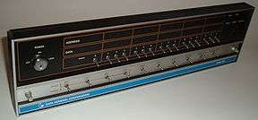
Front panel layout
As was the convention of the day, most Nova models provided a front panel console to control and monitor CPU functions. Models prior to the Nova 3 all relied on a canonical front panel layout, as shown in the Nova 840 panel photo above. The layout contained a keyed power switch, two rows of address and data display lamps, a row of data entry switches, and a row of function switches that activated various CPU functions when pressed. The address lamps always displayed the current value of the program counter, in binary. The data lamps displayed various values depending on which CPU function was active at the moment. To the left of the leftmost data lamp, an additional lamp displayed the current value of the carry bit. On most models the lamps were incandescent lamps which were soldered to the panel board; replacing burned-out lamps was a bane of existence for Data General field service engineers.
Each of the data switches controlled the value of one bit in a 16-bit value, and per Data General convention, they were numbered 0-15 from left to right. The data switches provided input to the CPU for various functions, and could also be read by a running program using the READS assembly language instruction. To reduce panel clutter and save money, the function switches were implemented as two-way momentary switches. When a function switch lever was lifted, it triggered the function whose name was printed above the switch on the panel; when the lever was pressed down, it activated the function whose name appeared below the switch. The switch lever returned to a neutral position when released.
Referencing the Nova 840 photo, the first four switches from the left performed the EXAMINE and DEPOSIT functions for the four accumulators. Pressing EXAMINE on one of these caused the current value of the accumulator to be displayed in binary by the data lamps. Pressing DEPOSIT transferred the binary value represented by the current settings of the data switches to the accumulator.
Going to the right, the next switch was the RESET/STOP switch. Pressing STOP caused the CPU to halt after completing the current instruction. Pressing RESET caused the CPU to halt immediately, cleared a number of CPU internal registers, and sent an I/O reset signal to all connected devices. The switch to the right of that was the START/CONTINUE switch. Pressing CONTINUE caused the CPU to resume executing at the instruction currently pointed at by the program counter. Pressing START transferred the value currently set in data switches 1-15 to the program counter, and then began executing from there.
The next two switches provided read and write access to memory from the front panel. Pressing EXAMINE transferred the value set in data switches 1-15 to the program counter, fetched the value in the corresponding memory location, and displayed its value in the data lamps. Pressing EXAMINE NEXT incremented the program counter and then performed an examine operation on that memory location, allowing the user to step through a series of memory locations. Pressing DEPOSIT wrote the value contained in the data switches to the memory location pointed at by the program counter. Pressing DEPOSIT NEXT first incremented the program counter and then deposited to the pointed-to memory location.
The INST STEP function caused the CPU to execute one instruction, at the current program counter location, and then halt. Since the program counter would be incremented as part of the instruction execution, this allowed the user to single-step through a program. MEMORY STEP, a misnomer, caused the CPU to run through a single clock cycle and halt. This was of little use to users and was generally only used by field service personnel for diagnostics.
PROGRAM LOAD was the mechanism usually used to boot a Nova. When this switch was triggered, it caused the 32-word boot ROM to be mapped over the first 32 words of memory, set the program counter to 0, and started the CPU. The boot ROM contained code that would read 256 words (512) bytes of code from a selected I/O device into memory and then transfer control to the read-in code. The data switches 8-15 were used to tell the boot ROM which I/O channel to boot from. If switch 0 was off, the boot ROM would assume the device was a polled device (e.g., the paper tape reader) and run a polled input loop until 512 bytes had been read. If switch 0 was on, the boot room assumed the device was a DMA-capable device and it initiated a DMA data transfer. The boot ROM was not smart enough to position the device prior to initiating the transfer. This was a problem when rebooting after a crash; if the boot device was a disk drive, its heads had likely been left on a random cylinder. They had to be repositioned to cylinder 0, where RDOS wrote the first-level boot block, in order for the boot sequence to work. Conventionally this was done by cycling the drive through its load sequence, but users who got frustrated with the wait time (up to 5 minutes depending on the drive model) learned how to input from the front panel a drive "recalibrate" I/O code and single-step the CPU through it, an operation that took an experienced user only a few seconds.
The power switch was a 3-way keyed switch with positions marked OFF, ON, and LOCK. In the OFF position all power was removed from the CPU. Turning the key to ON applied power to the CPU. However, unlike current CPUs, the CPU did not start automatically when power was applied; the user had to use PROGRAM LOAD or some other method to start the CPU and initiate the boot sequence. Turning the switch to LOCK disabled the front panel function switches; by turning the switch to LOCK and removing the key, the user could render the CPU resistant to tampering. On systems with magnetic core memory, the LOCK position also enabled the auto power failure recovery function. The key could be removed in the OFF or LOCK positions.
Performance
The Nova 1200 executed core memory access instructions (LDA and STA) in 2.55 microseconds (μs). Use of read only memory saved 0.4 μs. Accumulator instructions (ADD, SUB, COM, NEG, etc.) took 1.55 μs, MUL 2.55 μs, DIV 3.75 μs, ISZ 3.15-4.5 μs.[2] On the later Eclipse MV/6000, LDA and STA took 0.44 μs, ADD, etc. took 0.33 μs, MUL 2.2 μs, DIV 3.19 μs, ISZ 1.32 μs, FAD 5.17 μs, FMMD 11.66 μs.[3]
Assembly language examples
Hello world program
This is a minimal programming example in Nova assembly language. It is designed to run under RDOS and prints the string “Hello, world.” on the console.
    ; a "hello, world" program for Nova running RDOS
    ; uses PCHAR system call
    .titl hello
    .nrel
    .ent start

 start:
 dochar:
    lda    0,@pmsg  ; load ac0 with next character,
    mov#   0,0,snr  ; test ac0; skip if nonzero (don't load result)
    jmp    done
    .systm
    .pchar          ; print first
    jmp    er       ; skipped if OK
    movs   0,0      ; swap bytes
    .systm
    .pchar          ; print second
    jmp    er       ; skipped if OK
    isz    pmsg     ; point to next character
    jmp    dochar   ; go around again

 done:
    .systm          ; normal exit
    .rtn
 er:
    .systm          ; error exit
    .ertn
    halt

 pmsg:
    .+1             ; pointer to first character of string
                    ; note bytes are packed right-to-left by default
                    ; <15><12> denotes a CR LF pair.
    .txt /Hello, world.<15><12>/
    0               ; flag word to end string

    .end start
16-bit multiplication
Basic models of the Nova came without built-in hardware multiply and divide capability, to keep prices competitive. The following routine multiplies two 16-bit words to produce a 16-bit word result (overflow is ignored). It demonstrates combined use of ALU op, shift, and test (skip). Note that when this routine is called by jsr, AC3 holds the return address. This is used by the return instruction jmp 0,3. An idiomatic way to clear an accumulator is sub 0,0. Other single instructions can be arranged to load a specific set of useful constants (e.g. -2, -1, or +1).
 mpy:	; multiply AC0 <- AC1 * AC2, by Toby Thain

 	sub 0,0		; clear result
 mbit:	movzr 1,1,szc	; shift multiplier, test lsb
 	add 2,0		; 1: add multiplicand
 	movzl 2,2,szr	; shift and test for zero
 	jmp mbit	; not zero, do another bit
 	jmp 0,3		; return
Binary print accumulator
The following routine prints the value of AC1 as a 16 digit binary number, on the RDOS console. It reveals further quirks of the Nova instruction set. For instance, there is no instruction to load an arbitrary “immediate” value into an accumulator (although memory reference instructions do encode such a value to form an effective address). Accumulators must generally be loaded from initialized memory locations (e.g. n16). Other contemporary machines such as the PDP-11, and practically all modern architectures, allow for immediate loads, although many such as ARM restrict the range of values that can be loaded immediately.
Because the RDOS .systm call macro implements a jsr, AC3 is overwritten by the return address for the .pchar function. Therefore, a temporary location is needed to preserve the return address of the caller of this function. For a recursive or otherwise re-entrant routine, a stack, hardware if available, software if not, must be used instead. The return instruction becomes jmp @ retrn which exploits the Nova's indirect addressing mode to load the return PC.
The constant definitions at the end show two assembler features: the assembler radix is octal by default (20 = sixteen), and character constants could be encoded as e.g. "0.
 pbin:  ; print AC1 on console as 16 binary digits, by Toby Thain

        sta     3,retrn     ; save return addr
        lda     2,n16       ; set up bit counter
 loop:  lda     0,chr0      ; load ASCII '0'
        movzl   1,1,szc     ; get next bit in carry
        inc     0,0         ; bump to '1'
        .systm
        .pchar              ; AC0-2 preserved
        jmp     err         ; if error
        inc     2,2,szr     ; bump counter
        jmp     loop        ; loop again if not zero
        lda     0,spc       ; output a space
        .systm
        .pchar
        jmp     err         ; if error
        jmp     @retrn

 spc:   " ;that's a space
 chr0:  "0
 n16:   -20
 retrn: 0
Emulating a Data General Nova
Nova assembly language programs can be run under Bob Supnik’s SIMH emulator, in RDOS. Of the above examples, only Hello, world is a complete program. It includes the necessary directives for a successful assembly and generation of a runnable program.
Stepwise instructions
Start the Nova emulation and boot RDOS following th e instructions under “Nova and Eclipse RDOS” in the file src/simh_swre.txt of the simh distribution. After booting, RDOS’ command prompt, R, should appear on the screen.
- Before the first assembly on a newly setup RDOS system, the macro assembler’s default symbol definitions need to be configured using the following command:
mac/s nbid osid nsid paru - Create the assembly source file under RDOS:
xfer/a $tti test.sr(the xfer command will accept input at the console and copy it to a disk file named test.sr; after entering the command, copy and paste (or type in) a complete assembly language program, and finish with control-Z). - Next, run the macro assembler on test.sr to create the object file test.rb:
mac/l test(the /l [slash-ell] option enables the listing file test.ls, which can be copied to the console using the commandtype test.ls). - The relocatable loader, rldr, takes the object file and creates the executable test.sv :
rldr test - To run the program, type
test
Before going further with serious experimentation, it can be convenient to check one’s programs at the PC using a suitable cross-assembler, such as the portable PDP-8/DG Nova cross-assembler listed in the External links section, before attempting execution in the RDOS environment.
RDOS hints
- To have a directory listing of all files with the base name test, type
list test.-(note the hyphen, RDOS’ wildcard character) - Delete files with
delete(this might be needed because xfer won’t replace an existing file) - A running program can usually be interrupted with Control-A
- To exit RDOS, type
release %mdir% - Quit simh at its prompt with
q
Facts
The Canadian Broadcasting Corporation in Montreal used the Nova 1200 for channel play-out automation up until the late 80's. It was then replaced with refurbished Nova 4 units and these were in use until the mid 90's.
References
- ↑ Hey, Tony; Hey, Anthony; Pápay, Gyuri (2014). The Computing Universe: A Journey through a Revolution. p. 165.
- ↑ Technical Manual Nova 1200, Data General 015-000002, 1971, p.1-4
- ↑ Eclipse MV/6000 Principles of Operation, Data General 014-000648, 1980, App. F
External links
- Bob Supnik’s SimH project – Includes a basic Nova emulator in a user-modifiable package
- The portable C compiler includes a NOVA target.
- Novas Are Forever (SimuLogic’s) website – Attempts to archive everything DG plus provide free and commercial products
- A portable PDP-8 and DG Nova cross-assembler
- Carl Friend’s Minicomputer Museum – Describes the Nova instruction set in detail