Zilog Z80
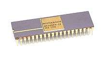
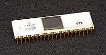
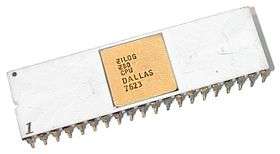 An early Z80 microprocessor, manufactured in June 1976 according to the date stamp. | |
| Produced | From March 1976 to present |
|---|---|
| Common manufacturer(s) | |
| Max. CPU clock rate | 2.5 MHz to 8 MHz with CMOS variant up to 20 MHz |
The Z80 CPU is an 8-bit based microprocessor. It was introduced by Zilog in 1976 as the startup company's first product. The Z80 was conceived by Federico Faggin in late 1974 and developed by him and his then 11 employee Zilog from early 1975 until March 1976, when the first fully working samples were delivered. With the revenue from the Z80, the company could then build its own chip factories and grow to over a thousand employees over the following two years.[2]
The Zilog Z80 was a software compatible extension and enhancement of the Intel 8080 and, like it, was mainly aimed at embedded systems. According to the designers, the primary targets for the Z80 CPU (and its optional support and peripheral ICs[3]) were products like intelligent terminals, high end printers and advanced cash registers as well as telecom equipment, industrial robots and other kinds of automation equipment.
The Z80 was officially introduced on the market in July 1976 and came to be widely used also in general desktop computers using CP/M and other operating systems as well as in the home computers of the 1980s. It was also common in military applications, musical equipment, such as synthesizers, and in the computerized coin operated video games of the late 1970s and early 1980, the arcade machines or video game arcade cabinets.
In the early 1980s, the Z80 was the most commonly used CPU of all time, and, along with the MOS Technology 6502 family, dominated the home computer market from the late 1970s to the mid 1980s.[4][5]
Zilog licensed the Z80 to the US based Synertek and Mostek, that had helped them with initial production, as well as to a Europan second source manufacturer, SGS. The design was copied also by several Japanese, East European and Russian manufacturers.[6] This enabled the Z80 to gain acceptance in the world market since large companies like NEC, Toshiba, Sharp, and Hitachi, started to manufacture the device (or their own Z80 compatible designs). In recent decades Zilog has refocused on the ever-growing market for embedded systems (for which the original Z80 and the Z180 were designed) and the most recent Z80-compatible microcontroller family, the fully pipelined 24-bit eZ80 with a linear 16 MB address range, has been successfully introduced alongside the simpler Z180 and Z80 products.
History
The Z80 came about when physicist Federico Faggin left Intel at the end of 1974 to found Zilog with Ralph Ungermann. At Fairchild Semiconductor, and later at Intel, Faggin had been working on fundamental transistor and semiconductor manufacturing technology. He also developed the basic design methodology used for memories and microprocessors at Intel and led the work on the Intel 4004, the 8080 and several other ICs. Masatoshi Shima, the principal logic and transistor level-designer of the 4004 and the 8080 under Faggin's supervision, also joined the Zilog team.
By March 1976, Zilog had developed the Z80 as well as an accompanying assembler based development system for its customers, and by July 1976, this was formally launched onto the market.[7] (Some of the Z80 support and peripheral ICs were under development at this point, and many of them were launched during the following year.)
Early Z80s were manufactured by Synertek and Mostek, before Zilog had its own manufacturing factory ready, in late 1976. These companies were chosen because they could do the ion implantation needed to create the depletion-mode MOSFETs that the Z80 design used as load transistors in order to cope with a single 5 Volt power supply.[8]
Faggin designed the instruction set to be binary compatible with the Intel 8080[9][10] so that most 8080 code, notably the CP/M operating system and Intel's PL/M compiler for 8080 (as well as its generated code), would run unmodified on the new Z80 CPU. Masatoshi Shima designed most of the microarchitecture as well as the gate and transistor levels of the Z80 CPU, assisted by a small number of engineers and layout people.[11][12][13]
The Z80 offered many improvements over the 8080:[10]
- An enhanced instruction set[14] including single-bit addressing, shifts/rotates on memory and registers other than the accumulator, program looping, block move, block input/output (I/O), and byte search instructions[15] The Z80 also incorporated an overflow flag and had better support for signed 8- and 16-bit quantities.[16]
- New IX and IY index registers with instructions for direct base+offset addressing
- A better interrupt system
- A more automatic and general vectorized interrupt system, mode 2, primarily intended for Zilog's line of counter/timers, DMA and communications controllers, as well as a fixed vector interrupt system, mode 1, for simple systems with minimal hardware (with mode 0 being the 8080-compatible mode).[17]
- A non maskable interrupt (NMI) which can be used to respond to power down situations and/or other high priority events (and allowing a minimalistic Z80 system to easily implement a two-level interrupt scheme in mode 1).
- Two separate register files, which could be quickly switched, to speed up response to interrupts such as fast asynchronous event handlers or a multitasking dispatcher. Although they were not intended as extra registers for general code, they were nevertheless used that way in some applications.[18]
- Less hardware required for power supply, clock generation and interface to memory and I/O
- Single 5-volt power supply (the 8080 needed -5 V/+5 V/+12 V).
- Single-phase 5 V clock (the 8080 needed a high-amplitude (9 to 12 volt) non-overlapping two-phase clock).
- A built-in DRAM refresh mechanism that would otherwise have to be provided by external circuitry.[19]
- Non-multiplexed buses (the 8080 had state-signals multiplexed onto the data bus).
- A special reset function which clears only the program counter so that a single Z80 CPU could be used in a development system such as an in-circuit emulator.[20]
The Z80 took over from the 8080 and its offspring, the 8085, in the processor market,[21] and became one of the most popular 8-bit CPUs.[4][5] Perhaps a key to the initial success of the Z80 was the built-in DRAM refresh, and other features which allowed systems to be built with fewer support chips (Z80 embedded systems typically use static RAM and hence do not need this refresh).
For the original NMOS design, the specified upper clock frequency limit increased successively from the introductory 2.5 MHz, via the well known 4 MHz (Z80A), up to 6 (Z80B) and 8 MHz (Z80H).[22][23] CMOS versions were also developed with specified upper frequency limits ranging from 4 MHz up to 20 MHz for the version sold today. The CMOS versions also allowed low-power sleep with internal state retained, having no lower frequency limit.[24] The fully compatible derivatives HD64180/Z180[25][26] and eZ80 are currently specified for up to 33 and 50 MHz respectively.
Design
Programming model and register set
The programming model and register set are conventional and similar to the related x86 family. The 8080 compatible registers AF, BC, DE, HL are duplicated as two separate banks in the Z80,[27] where the processor can quickly switch from one bank to the other;[28] a feature useful for speeding up responses to single-level, high-priority interrupts. This feature was present in the Datapoint 2200 but was not implemented by Intel in the 8008. The dual register-set makes sense as the Z80 (like most microprocessors at the time) was really intended for embedded use, not for personal computers, or the yet-to-be invented home computers. According to one of the designers, Masatoshi Shima, the market focus was on high performance printers, high-end cash registers, and intelligent terminals. The two register sets also turned out to be quite useful for heavily optimized manual assembly-language coding.
Registers
| The Z80 registers | ||||||||||||||||||||||||||||||||||||||||||||||||||||||||||||||||||||||||||||||||||||||||||||||||||||||||||||||||||||||||||||||||||||||||||||||||||||||||||||||||||||||||||||||||||||||||||||||||||||||||||||||||||||||||||||||||||||||||||||||||||||||||||||||||||||||||||||||||||||||||||||||||||||||||||||||||||||||||||||||||||||||||||||||||||||||||||||||||||||||||||||||||||||||
| ||||||||||||||||||||||||||||||||||||||||||||||||||||||||||||||||||||||||||||||||||||||||||||||||||||||||||||||||||||||||||||||||||||||||||||||||||||||||||||||||||||||||||||||||||||||||||||||||||||||||||||||||||||||||||||||||||||||||||||||||||||||||||||||||||||||||||||||||||||||||||||||||||||||||||||||||||||||||||||||||||||||||||||||||||||||||||||||||||||||||||||||||||||||
As on the 8080, 8-bit registers are typically paired to provide 16-bit versions. The 8080 compatible registers[29] are:
-
AF: 8-bit accumulator (A) and flag bits (F) carry, zero, minus, parity/overflow, half-carry (used for BCD), and an Add/Subtract flag (usually called N) also for BCD -
BC: 16-bit data/address register or two 8-bit registers -
DE: 16-bit data/address register or two 8-bit registers -
HL: 16-bit accumulator/address register or two 8-bit registers -
SP: stack pointer, 16 bits -
PC: program counter, 16 bits
The new registers introduced with the Z80 are:
-
IX: 16-bit index or base register for 8-bit immediate offsets -
IY: 16-bit index or base register for 8-bit immediate offsets -
I: interrupt vector base register, 8 bits -
R: DRAM refresh counter, 8 bits (msb does not count) -
AF': alternate (or shadow) accumulator and flags (toggled in and out with EX AF,AF' ) -
BC',DE'andHL': alternate (or shadow) registers (toggled in and out with EXX) - Four bits of interrupt status and interrupt mode status
There is no direct access to the alternate registers; instead, two special instructions, EX AF,AF' and EXX,[29] each toggles one of two multiplexer flip-flops; this enables fast context switches for interrupt service routines: EX AF, AF' may be used alone (for really simple and fast interrupt routines) or together with EXX to swap the whole BC, DE, HL set; still much faster than pushing the same registers on the stack (slower, lower priority, or multi level interrupts normally use the stack to store registers).
The refresh register, R, increments each time the CPU fetches an opcode (or opcode prefix) and has therefore no simple relationship with program execution. This has sometimes been used to generate pseudorandom numbers in games, and also in software protection schemes. It has also been employed as a "hardware" counter in some designs; an example of this is the ZX81, which lets it keep track of character positions on the TV screen by triggering an interrupt at wrap around (by connecting INT to A6).
The interrupt vector register, I, is used for the Z80 specific mode 2 interrupts (selected by the IM 2 instruction). It supplies the high byte of the base address for a 128-entry table of service routine addresses which are selected via an index sent to the CPU during an interrupt acknowledge cycle; this index is simply the low byte part of the pointer to the tabulated indirect address pointing to the service routine.[17] The pointer identifies a particular peripheral chip and/or peripheral function or event, where the chips are normally connected in a so-called daisy chain for priority resolution. Like the refresh register, this register has also sometimes been used creatively; in interrupt modes 0 and 1 (or in a system not using interrupts) it can be used as simply another 8-bit data register.
The instructions LD A,R and LD A,I affect the Z80 flags register, unlike all the other LD (load) instructions. The Sign (bit 7) and Zero (bit 6) flags are set according to the data loaded from the Refresh or Interrupt source registers. For both instructions, the Parity/Overflow flag (bit 2) is set according to the current state of the IFF2 flip-flop.[30]
Z80 assembly language
Datapoint 2200 and Intel 8008
The first Intel 8008 assembly language was based on a very simple (but systematic) syntax inherited from the Datapoint 2200 design. This original syntax was later transformed into a new, somewhat more traditional, assembly language form for this same original 8008 chip. At about the same time, the new assembly language was also extended to accommodate the added addressing possibilities in the more advanced Intel 8080 chip (the 8008 and 8080 shared a language subset without being binary compatible; however, the 8008 was binary compatible with the Datapoint 2200).
In this process, the mnemonic L, for LOAD, was replaced by various abbreviations of the words LOAD, STORE and MOVE, intermixed with other symbolic letters. The mnemonic letter M, for memory (referenced by HL), was lifted out from within the instruction mnemonic to become a syntactically freestanding operand, while registers and combinations of registers became very inconsistently denoted; either by abbreviated operands (MVI D, LXI H and so on), within the instruction mnemonic itself (LDA, LHLD and so on), or both at the same time (LDAX B, STAX D and so on).
| Datapoint 2200 & i8008 | i8080 | Z80 | i8086/i8088 |
|---|---|---|---|
| before ~1973 | ~1974 | 1976 | 1978 |
LBC |
MOV B,C |
LD B,C |
MOV BL,CL |
-- |
LDAX B |
LD A,(BC) |
MOV AL,[BX] |
LAM |
MOV A,M |
LD A,(HL) |
MOV AL,[BP] |
LBM |
MOV B,M |
LD B,(HL) |
MOV BL,[BP] |
-- |
STAX D |
LD (DE),A |
MOV [DX],AL[31] |
LMA |
MOV M,A |
LD (HL),A |
MOV [BP],AL |
LMC |
MOV M,C |
LD (HL),C |
MOV [BP],CL |
LDI 56 |
MVI D,56 |
LD D,56 |
MOV DL,56 |
LMI 56 |
MVI M,56 |
LD (HL),56 |
MOV byte ptr [BP],56 |
-- |
LDA 1234 |
LD A,(1234) |
MOV AL,[1234] |
-- |
STA 1234 |
LD (1234),A |
MOV [1234],AL |
-- |
-- |
LD B,(IX+56) |
MOV BL,[SI+56] |
-- |
-- |
LD (IX+56),C |
MOV [SI+56],CL |
-- |
-- |
LD (IY+56),78 |
MOV byte ptr [DI+56],78 |
-- |
LXI B,1234 |
LD BC,1234 |
MOV BX,1234 |
-- |
LXI H,1234 |
LD HL,1234 |
MOV BP,1234 |
-- |
SHLD 1234 |
LD (1234),HL |
MOV [1234],BP |
-- |
LHLD 1234 |
LD HL,(1234) |
MOV BP,[1234] |
-- |
-- |
LD BC,(1234) |
MOV BX,[1234] |
-- |
-- |
LD IX,(1234) |
MOV SI,[1234] |
Illustration of four syntaxes, using samples of equivalent, or (for 8086) very similar, load and store instructions.[32] The Z80 syntax uses parentheses around an expression to indicate that the value should be used as a memory address (as mentioned below), while the 8086 syntax uses brackets instead of ordinary parentheses for this purpose. Both Z80 and 8086 use the + sign to indicate that a constant is added to a base register to form an address
New syntax
Because Intel had a copyright on their assembly mnemonics,[33] a new assembly syntax had to be developed for the Z80. This time a more systematic approach was used:
- All registers and register pairs are explicitly denoted by their full names
- Parentheses are consistently used to indicate "memory contents at" (constant address or variable pointer dereferencing) with the exception of some jump instructions.[34]
- All load and store instructions use the same mnemonic name, LD, for LOAD (a return to the simplistic Datapoint 2200 vocabulary); other common instructions, such as ADD and INC, use the same mnemonic regardless of addressing mode or operand size. This is possible because the operands themselves carry enough information.
These principles made it straightforward to find names and forms for all new Z80 instructions, as well as orthogonalizations of old ones, such as LD BC,(1234).
Apart from naming differences, and despite a certain discrepancy in basic register structure, the Z80 and 8086 syntax are virtually isomorphic for a large portion of instructions. Only quite superficial similarities (such as the word MOV, or the letter X, for extended register) exist between the 8080 and 8086 assembly languages, although 8080 programs can be assembled into 8086 object code using a special assembler or translated to 8086 assembly language by a translator program.[35][36]
Instruction set and encoding
The Z80 uses 252 out of the available 256 codes as single byte opcodes ("root instruction"); the four remaining codes are used extensively as opcode prefixes:[37] CB and ED enable extra instructions and DD or FD selects IX+d or IY+d respectively (in some cases without displacement d) in place of HL. This scheme gives the Z80 a large number of permutations of instructions and registers; Zilog categorizes these into 158 different "instruction types", 78 of which are the same as those of the Intel 8080[37] (allowing operation of most 8080 programs on a Z80). The Zilog documentation further groups instructions into the following categories:
- 8-bit arithmetic and logic operations
- 16-bit arithmetic
- 8-bit load
- 16-bit load
- Bit set, reset, and test
- Call, return, and restart
- Exchange, block transfer, and search
- General purpose arithmetic and CPU control
- Input and output
- Jump
- Rotate and shift
No multiply instruction is available in the original Z80.[38] Different sizes and variants of additions, shifts, and rotates have somewhat differing effects on flags because most[39] of the flag-changing properties of the 8080 were copied.
The Z80 has four new LD instructions that can load the DE and BC register pairs from memory, and load memory from these two register pairs -- unlike the 8080.[40] As on the 8080, load instructions do not affect the flags (except for the special purpose I and R register loads). A quirk (common with the 8080) of the register-to-register load instructions is that each of the 8-bit registers can be loaded from themselves (e.g. LD A,A). This is effectively a NOP.
Unlike the 8080, the Z80 can jump to a relative address using a signed 8-bit displacement. Only the Zero and Carry flags can be tested for these new two-byte JR instructions.
A two-byte instruction specialized for program looping is new to the Z80. DJNZ (Decrement Jump if Non-Zero) takes a signed 8-bit displacement as an immediate operand. The B register is decremented. If the result is nonzero then program execution jumps relative to the address of the PC plus the displacement. The flags remain unaltered. To perform an equivalent loop on an 8080 would require separate decrement and jump (to a two-byte absolute address) instructions, and the flag register would be altered.
The index register (IX/IY) instructions can be useful for accessing data organised in fixed heterogenous structures (such as records) or at fixed offsets relative a variable base address (as in recursive stack frames) and can also reduce code size by removing the need for multiple short instructions using non-indexed registers. However, although they may save speed in some contexts when compared to long/complex "equivalent" sequences of simpler operations, they incur a lot of additional CPU time (e.g. 19 T-states to access one indexed memory location vs. as little as 11 to access the same memory using HL and INCrement it to point to the next). Thus, for simple or linear accesses of data, IX and IY tend to be slower. Still, they may be useful in cases where the 'main' registers are all occupied, by removing the need to save/restore registers. Their officially undocumented 8-bit halves (see below) can be especially useful in this context, for they incur less slowdown than their 16-bit parents. Similarly, instructions for 16-bit additions are not particularly fast (11 clocks) in the original Z80; nonetheless, they are about twice as fast as performing the same calculations using 8-bit operations, and equally important, they reduce register usage.
The 10-year-newer microcoded Z180 design could initially afford more "chip area", permitting a slightly more efficient implementation (using a wider ALU, among other things); similar things can be said for the Z800, Z280, and Z380. However, it was not until the fully pipelined eZ80 was launched in 2001 that those instructions finally became approximately as cycle-efficient as it is technically possible to make them, i.e. given the Z80 encodings combined with the capability to do an 8-bit read or write every clock cycle.
Undocumented instructions
The index registers, IX and IY, were intended as flexible 16 bit pointers, enhancing the ability to manipulate memory, stack frames and data structures. Officially, they were treated as 16-bit only. In reality, they were implemented as a pair of 8-bit registers,[41] in the same fashion as the HL register, which is accessible either as 16 bits or separately as the High and Low registers. Even the binary opcodes (machine language) were identical, but preceded by a new opcode prefix.[42] Zilog published the opcodes and related mnemonics for the intended functions, but did not document the fact that every opcode that allowed manipulation of the H and L registers was equally valid for the 8 bit portions of the IX and IY registers. As an example, the opcode 26h followed by an immediate byte value (LD H,n) will load that value into the H register. Preceding this two-byte instruction with the IX register's opcode prefix, DD, would instead result in the most significant 8 bits of the IX register being loaded with that same value. A notable exception to this would be instructions similar to LD H,(IX+d) which make use of both the HL and IX or IY registers in the same instruction;[42] in this case the DD prefix is only applied to the (IX+d) portion of the instruction.
There are several other undocumented instructions as well.[43] Undocumented or illegal opcodes are not detected by the Z80 and have various effects, some of which are useful. However, as they are not part of the formal definition of the instruction set, different implementations of the Z80 are not guaranteed to work the same way for every undocumented opcode.
Bugs
The OTDR instruction doesn't conform to the Z80 documentation. Both OTDR and OTIR are supposed to leave the carry C unaffected. OTIR functions correctly; however, during the execution of the OTDR instruction, the carry takes the results of a spurious compare between the accumulator and what has last been output by the OTDR instruction.
Example code
The following Z80 assembly source code is for a subroutine named memcpy that copies a block of data bytes of a given size from one location to another. Important: The example code does not handle a certain case where the destination block overlaps the source; a fatal bug. The sample code is extremely inefficient, intended to illustrate various instruction types, rather than best practices for speed. In particular, the Z80 has a single instruction that will execute the entire loop (LDIR). The data block is copied one byte at a time, and the data movement and looping logic utilizes 16-bit operations. Note that the assembled code is binary-compatible with the Intel 8080 and 8085 CPUs.
 1000
 1000
 1000 78
 1001 B1
 1002 C8
 1003 1A
 1004 77
 1005 13
 1006 23
 1007 0B
 1008 C3 00 10
 100B
|
 ; memcpy --
 ; Copy a block of memory from one location to another.
 ;
 ; Entry registers
 ;      BC - Number of bytes to copy
 ;      DE - Address of source data block
 ;      HL - Address of target data block
 ;
 ; Return registers
 ;      BC - Zero

             org     1000h       ;Origin at 1000h
 memcpy      public
 loop        ld      a,b         ;Test BC,
             or      c           ;If BC = 0,
             ret     z           ;Return
             ld      a,(de)      ;Load A from (DE)
             ld      (hl),a      ;Store A into (HL)
             inc     de          ;Increment DE
             inc     hl          ;Increment HL
             dec     bc          ;Decrement BC
             jp      loop        ;Repeat the loop
             end
|
Instruction execution
Each instruction is executed in steps that are usually termed machine cycles (M-cycles), each of which can take between three and six clock periods (T-cycles).[44] Each M-cycle corresponds roughly to one memory access and/or internal operation. Many instructions actually end during the M1 of the next instruction which is known as a fetch/execute overlap.
| Total
M-cycles |
instruction | M1 | M2 | M3 | M4 | M5 | M6 |
|---|---|---|---|---|---|---|---|
| 1[45] | INC BC |
opcode | |||||
| 2[46] | ADD A,n |
opcode | n | ||||
| 3[47] | ADD HL,DE |
opcode | internal | internal | |||
| 4[48] | SET b,(HL) |
prefix | opcode | R(HL), set | W(HL) | ||
| 5[49] | LD (IX+d),n |
prefix | opcode | d | n,add | W(IX+d) | |
| 6[50] | INC (IY+d) |
prefix | opcode | d | add | R(IY+d),inc | W(IY+d) |
The Z80 machine cycles are sequenced by an internal state machine which builds each M-cycle out of 3, 4, 5 or 6 T-cycles depending on context. This avoids cumbersome asynchronous logic and makes the control signals behave consistently at a wide range of clock frequencies. It also means that a higher frequency crystal must be used than without this subdivision of machine cycles (approximately 2–3 times higher). It does not imply tighter requirements on memory access times, however, as a high resolution clock allows more precise control of memory timings and memory therefore can be active in parallel with the CPU to a greater extent (i.e. sitting less idle), allowing more efficient use of available memory bandwidth.
One central example of this is that, for opcode fetch, the Z80 combines two full clock cycles into a memory access period (the M1-signal). In the Z80 this signal therefore lasts for a much larger (relative) part of the typical instruction execution time than in a more asynchronous processor design such as the 6800, 6502, or similar, where this period would typically last only a (rather imprecise) fraction (typically 30-40%) of a clock cycle. With memory chip affordability (i.e. access times around 450-250 ns in the 1980s) typically determining the fastest possible access time, this meant that such designs were locked to a significantly longer clock cycle (i.e. lower internal clock speed) than the Z80.
Memory, especially EPROM, but also Flash, were generally slow as compared to the state machine sub-cycles (clock cycles) used in contemporary microprocessors. The shortest machine cycle that could safely be used in embedded designs has therefore often been limited by memory access times, not by the maximum CPU frequency (especially so during the home computer era). However, this relation has slowly changed during the last decades, particularly regarding SRAM; cacheless, single-cycle designs such as the eZ80 have therefore become much more meaningful recently.
The content of the refresh register R is sent out on the lower half of the address bus along with a refresh control signal while the CPU is decoding and executing the fetched instruction. During refresh the contents of the Interrupt register I are sent out on the upper half of the address bus.[51]
Compatible peripherals
Zilog introduced a number of peripheral parts for the Z80, which all supported the Z80's interrupt handling system and I/O address space. These included the Counter/Timer Channel (CTC),[52] the SIO (Serial Input Output), the DMA (Direct Memory Access), the PIO (Parallel Input-Output) and the DART (Dual Asynchronous Receiver Transmitter). As the product line developed, low-power, high-speed and CMOS versions of these chips were produced.
Like the 8080, 8085 and 8086 processors, but unlike processors such as the Motorola 6800 and MOS Technology 6502, the Z80 and 8080 had a separate control line and address space for I/O instructions. While some Z80-based computers such as the Osborne 1 used "Motorola-style" memory mapped input/output devices, usually the I/O space was used to address one of the many Zilog peripheral chips compatible with the Z80. Zilog I/O chips supported the Z80's new mode 2 interrupts which simplified interrupt handling for large numbers of peripherals.
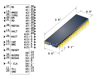
The Z80 was officially described as supporting 16-bit (64 KB) memory addressing, and 8-bit (256 ports) I/O-addressing. All I/O instructions actually assert the entire 16-bit address bus. OUT (C),reg and IN reg,(C) places the contents of the entire 16 bit BC register on the address bus;[53] OUT (n),A and IN A,(n) places the contents of the A register on b8-b15 of the address bus and n on b0-b7 of the address bus. A designer could choose to decode the entire 16 bit address bus on I/O operations in order to take advantage of this feature, or use the high half of the address bus to select subfeatures of the I/O device. This feature has also been used to minimise decoding hardware requirements, such as in the Amstrad CPC/PCW and ZX81.
Second sources and derivatives
Second sources

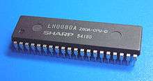
Mostek, who produced the first Z80 for Zilog, offered it as second-source as MK3880. SGS-Thomson (now STMicroelectronics) was a second-source, too, with their Z8400. Sharp and NEC developed second sources for the NMOS Z80, the LH0080 and µPD780C respectively. The µPD780C was used in the Sinclair ZX80 and ZX81, original versions of the ZX Spectrum, and several MSX computers, and in musical synthesizers such as Oberheim OB-8 and others. The LH0080 was used in various home computers and personal computers made by Sharp and other Japanese manufacturers, including Sony MSX computers, and a number of computers in the Sharp MZ series.[54]
Toshiba made a CMOS-version, the TMPZ84C00, which is believed (but not verified) to be the same design also used by Zilog for its own CMOS Z84C00. There were also Z80-chips made by GoldStar (alias LG) and the BU18400 series of Z80-clones (including DMA, PIO, CTC, DART and SIO) in NMOS and CMOS made by ROHM Electronics.
In East Germany, an unlicensed clone of the Z80, known as the U880, was manufactured. It was very popular and was used in Robotron's and VEB Mikroelektronik Mühlhausen's computer systems (such as the KC85-series) and also in many self-made computer systems. In Romania another unlicensed clone could be found, named MMN80CPU and produced by Microelectronica, used in home computers like TIM-S, HC, COBRA.
Also, several clones of Z80 were created in the Soviet Union, notable ones being the T34BM1, also called КР1858ВМ1 (parallelling the Russian 8080-clone KR580VM80A). The first marking was used in pre-production series, while the second had to be used for a larger production. Though, due to the collapse of Soviet microelectronics in the late 1980s, there are many more T34BM1s than КР1858ВМ1s.
Derivatives
- Compatible with the original Z80
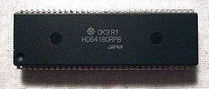
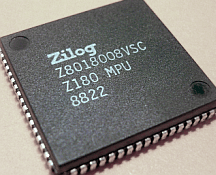
- Hitachi developed the HD64180, a microcoded and partially dynamic Z80 in CMOS, with on chip peripherals and a simple MMU giving a 1 MB address space. It was later second sourced by Zilog, initially as the Z64180, and then in the form of the slightly modified Z180[55] which has bus protocol and timings better adapted to Z80 peripheral chips. Z180 has been maintained and further developed under Zilog's name, the newest versions being based on the fully static S180/L180 core with very low power draw and EMI (noise).
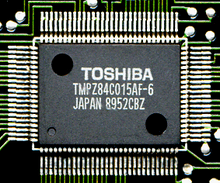
- Toshiba developed the 84 pin Z84013 / Z84C13 and the 100 pin Z84015 / Z84C15 series of "intelligent peripheral controllers", basically ordinary NMOS and CMOS Z80 cores with Z80 peripherals, watch dog timer, power on reset, and wait state generator on the same chip. Manufactured by Sharp as well as Toshiba. These products are today second sourced by Zilog.[56]
- The 32-bit Z80 compatible Zilog Z380, introduced 1994, is used mainly in telecom equipment.
- Zilog's fully pipelined Z80 compatible eZ80[57] with an 8/16/24-bit word length and a linear 16 MB address space was introduced in 2001. It exists in versions with on chip SRAM and/or flash memory, as well as with integrated peripherals. One variant has on chip MAC (media access controller), and available software include a TCP/IP stack. In contrast with the Z800 and Z280, there are only a few added instructions (primarily LEAs, PEAs, and variable-address 16/24-bit loads), but instructions are instead executed between 2 and 11 times as clock cycle efficient as on the original Z80 (with a mean value around 3-5 times). It is currently specified for clock frequencies up to 50 MHz.
- Kawasaki developed the binary compatible KL5C8400 which is approximately 1.2-1.3 times as clock cycle efficient as the original Z80 and can be clocked at up to 33 MHz. Kawasaki also produces the KL5C80A1x family, which has peripherals as well as a small RAM on chip; it is approximately as clock cycle efficient as the eZ80 and can be clocked at up to 10 MHz (2006).[58]
- The NEC uPD9002 was an hybrid CPU compatible with both Z80 and x86 families.
- The Chinese Actions Semiconductor's audio processor family of chips (ATJ2085 and others) contains a Z80-compatible MCU together with a 24-bit dedicated DSP processor.[59] These chips are used in many MP3 and media player products.
- The T80 (VHDL) and TV80 (Verilog) synthesizable soft cores are available from OpenCores.org.[60]
- Non-compatible
- The Toshiba TLCS 900 series of high volume (mostly OTP) microcontrollers are based on the Z80; they share the same basic BC,DE,HL,IX,IY register structure, and largely the same instructions, but are not binary compatible, while the previous TLCS 90 is Z80-compatible.[61]
- The NEC 78K series microcontrollers are based on the Z80; they share the same basic BC,DE,HL register structure, and has similar (but differently named) instructions; not binary compatible.
- Partly compatible
- Rabbit Semiconductor's Rabbit 2000/3000/4000 microprocessors/microcontrollers[62] are based on the HD64180/Z180 architecture, although they are not fully binary compatible.[63]
- No longer produced
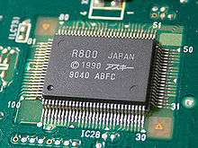
- The ASCII Corporation R800 was a fast 16-bit processor used in MSX TurboR computers; it was software, but not hardware compatible with the Z80 (signal timing, pinout & function of pins differ from the Z80).
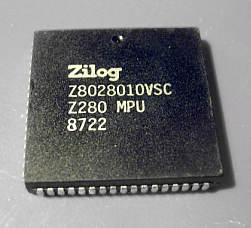
- Zilog's NMOS Z800 and CMOS Z280 were 16-bit Z80-implementations (before the HD64180 / Z180) with a 16 MB paged MMU address space; they added many orthogonalizations and addressing modes to the Z80 instruction set. Minicomputer features — such as user and system modes, multiprocessor support, on chip MMU, on chip instruction and data cache and so on — were seen rather as more complexity than as functionality and support for the (usually electronics-oriented) embedded systems designer, it also made it very hard to predict instruction execution times.
- Certain arcade games such as Pang/Buster Bros use an encrypted "Kabuki" Z80 CPU manufactured by VLSI Technology, where the decryption keys are stored in its internal battery-backed memory, to avoid piracy and illegal bootleg games.[64]
Notable uses
Desktop computers
During the late 1970s and early 1980s, the Z80 was used in a great number of fairly anonymous business-oriented machines with the CP/M operating system, a combination that dominated the market at the time.[65][66] Two well-known examples of Z80+CP/M business computers are the portable Osborne 1 and the Kaypro series. Research Machines manufactured the 380Z and 480Z microcomputers which were networked with a thin Ethernet type LAN and CP/NET in 1981. Other manufacturers of such systems included Televideo, Xerox (820 range) and a number of more obscure firms. Some systems used multi-tasking operating system software to share the one processor between several concurrent users.
In the U.S., the Radio Shack TRS-80, introduced in 1977, as well as the Models II, III, IV, and the proposed Model V, used the Z80. In the United Kingdom, Sinclair Research used the Z80 and Z80A in its ZX80, ZX81 and, ZX Spectrum home computers. Amstrad used them in their Amstrad CPC range and an early UK computer, the Nascom 1 and 2 also used the Z80. The Commodore 128 featured a Z80 processor alongside its MOS Technology 8502 processor for CP/M compatibility.[67] Other 6502 architecture computers on the market at the time, such as the BBC Micro, Apple II,[68] and the 6510 based Commodore 64,[69] could make use of the Z80 with an external unit, a plug-in card, or an expansion ROM cartridge. The Microsoft Z-80 SoftCard for the Apple II was a particularly successful add-on card and one of Microsoft's few hardware products of the era.
In 1981, Multitech (later to become Acer) introduced the Microprofessor I, a simple and inexpensive training system for the Z80 microprocessor. Currently, it is still manufactured and sold by Flite Electronics International Limited in Southampton, England.
Embedded systems and consumer electronics
The Zilog Z80 has long been a popular microprocessor in embedded systems and microcontroller cores,[29] where it remains in widespread use today.[4][70] The following list provides examples of such applications of the Z80, including uses in consumer electronics products.
Industry
- The IBM PC-XT's hard drive controller, which was actually an IBM adaptation of the Xebec 1410 SASI controller, but on a PC-XT bus, not a SASI bus.
- Office equipment such as matrix printers, fax machines, answering machines, and photocopiers are known examples.
- Industrial programmable logic controllers (PLCs) use the Z80 in CPU modules, for auxiliary functions such as analog I/O, or in communication modules.
- It has also been employed in robots, for example for speech recognition[71] and low level tasks such as servo processors in pick and place machines.
- RS-232 multiplexers connecting large numbers of old style "terminals" to minicomputers or mainframes used arrays of Z80 CPU/SIO boards.
- Applications such as TV broadcast vision mixers have used the Z80 for embedded real time subtasks.[72][73]
- It has also been used in Seagate Technology's and other manufacturers' hard disks.
- Credit card consoles controlling fuel pumps used Z80 CPU and PIOs (US patents 4930665, 4962462 and 5602745).
- Retail industry point-of-sale credit card terminals manufactured by VeriFone used the Z80 processor.
- Several PC expansion cards, such as Adaptecs SCSI boards, have been using the Z80/Z180 and peripheral chips.
- Z80/Z180/Z380 have been used in telecommunication equipment such as telephone switches and various kinds of modems.
- The Stofor message switch, used extensively by banks and brokers in the UK was Z80 based.
- Cash registers and store management systems
- Home automation, wireless sprinkler control and wireless mesh using the N8VEM open source homebrew system.
- Breathalyzer equipment used by law enforcement agencies.[74]
Consumer electronics
- Z80 was often used in coin-operated arcade games,[4] and was commonly used as the main CPU, sound or video coprocessors. Pac-Man arcade games feature a single Z80 as the main CPU,[75] and Frogger used two Z80 CPUs. Galaxian and arcade games such as King & Balloon and Check Man that use the Namco Galaxian boardset also use a Z80 as the main CPU.[76] Other Namco licensed arcade games such as Galaga and other games that use the Namco Galaga boardset such as Bosconian, Dig Dug, Xevious, and Super Xevious use three Z80 microprocessors running in parallel for the main CPU, graphics, and sound.[77] Later Sega System 16, 18, X, and Y; Capcom CPS1 and CPS2; SNK Neo Geo MVS use 68000 and Z80 combination as co processors or sound CPUs.
- It was also found in home video game consoles such as the ColecoVision,[78] Sega Master System[79] and Sega Game Gear video game consoles, as an audio and general-purpose co-processor in the Sega Genesis and as an audio controller and co-processor to the Motorola 68000 in the SNK Neo-Geo.
- Nintendo's Game Boy and Game Boy Color handheld game systems used an 8080-derived processor with some Z80 instructions added (CB prefix) as well as unique auto-increment/decrement addressing modes. The CPU was a Sharp Corporation LR35902[80] running at 4.19 MHz in the original and Pocket models, and 8.39 MHz in the Color model. This processor was later included in the Game Boy Advance / SP / Micro taking up a new role as a co-processor for backwards compatibility with Game Boy / Color games (except Micro) and to add legacy 8-bit sounds to supplement the digital samples in Game Boy Advance games.
- In Russia, Z80 and its clones were widely used in multi-functional land line phones with Caller ID.
- Various scientific and graphing calculators use the Z80, including the Texas Instruments TI-73, TI-81, TI-82, TI-83, TI-83+, TI-84+, TI-85 and TI-86 series.[81]
- The Ericsson GA628 mobile phone uses the Z80 CPU.[82]
- All the S1 MP3 Player type digital audio players use the Z80 instruction set.[83]
Musical instruments
- MIDI sequencers such as E-mu 4060 Polyphonic Keyboard and Sequencer, Zyklus MPS, and Roland MSQ700 were built around the Z80.
- MIDI controllers and switches such as Waldorf Midi-Bay MB-15 and others.
- Several polyphonic analog synthesizers used it for keyboard-scanning (also wheels, knobs, displays...) and D/A or PWM control of analog levels; in newer designs, sometimes sequencing and/or MIDI-communication. The Z80 was also often involved in the sound generation itself, implementing LFOs, envelope generators and so on. Known examples include:
- Sequential Circuits Prophet 5, Prophet 10,[84] Prophet 600, Six-Trak, Multitrak, MAX, and Split-8
- MemoryMoog six-voice synthesizer[85]
- Oberheim OB-8 eight-voice synthesizer with MIDI
- Roland Jupiter-8 eight-voice synthesizer
- Digital sampling synthesizers such as the Emulator I, Emulator II, and Akai S700 12-bit Sampler, as well as drum machines like the E-mu SP-12, E-mu SP-1200, E-mu Drumulator, and the Sequential Circuits Drumtraks, used Z80 processors.
- Many Lexicon reverberators (PCM70, LXP15, LXP1, MPX100) used one or more Z80s for user interface and LFO generation where dedicated hardware provided DSP functions.
- The ADA MP-1 and Digitech GSP 2101/2112/2120, MIDI controlled, vacuum tube, guitar pre-amplifiers.
See also
Footnotes
- ↑ Only in CMOS, National made no NMOS version, according to Oral History with Federico Faggin
- ↑ Source: Federico Faggin oral history.
- ↑ These were named the Z80 CTC (counter/timer), Z80 DMA (direct memory access), Z80 DART (dual asynchronous receiver-transmitter), Z80 SIO (synchronous communication controller), and Z80 PIO (parallel input/output)
- 1 2 3 4 Balch, Mark (2003-06-18). "Digital Fundamentals". Complete Digital Design: A Comprehensive Guide to Digital Electronics and Computer System Architecture. Professional Engineering. New York, New York: McGraw-Hill Professional. p. 122. ISBN 0-07-140927-0.
- 1 2 The Seybold report on professional computing. Seybold Publications. 1983.
In the 8-bit world, the two most popular microcomputers are the Z80 and 6502 computer chips.
- ↑ Zilog actually included several "traps" in the layout of the chip to try to delay this copying. According to Faggin, a NEC engineer later told him it had cost them several months of work, before they were able to get their μPD780 to function.
- ↑ Anderson 1994, p. 51
- ↑ Zilog manufactured the Z80 as well as most of their other products for many years until they sold their manufacturing plants and become the "fabless" company they are today.
- ↑ Anderson 1994, p. 57
- 1 2 Brock, Gerald W. (2003). The second information revolution. Harvard University Press. ISBN 978-0-674-01178-6.
- ↑ "History of the 8-bit: travelling far in a short time". InfoWorld. Vol. 4 no. 47. Palo Alto, CA: Popular Computing Inc. November 29, 1982. pp. 58–60. ISSN 0199-6649.
- ↑ Shima, Masatoshi; Federico Faggin; Ralph Ungermann (August 19, 1976). "Z-80 chip set heralds third microprocessor generation". Electronics. New York. 49 (17): 32–33 McGraw–Hill.
- ↑ CEO Federico Faggin was actually heavily involved in the chip layout work, together with two dedicated layout people. Faggin worked 80 hours a week in order to meet the tight schedule given by the financial investors, according to himself. (See Federico Faggin, oral history.)
- ↑ Mathur. Introduction to Microprocessors. p. 111. ISBN 978-0-07-460222-5.
The register architecture of the Z80 is more innovative than that of the 8085
- ↑ Ciarcia 1981, pp. 31,32
- ↑ Although the 8080 had 16-bit addition and 16-bit increment and decrement instructions, it had no explicit 16-bit subtraction, and therefore no possibilty to correctly set an overflow flag. The Z80 complemented this with the ADC HL,rr and SBC HL,rr instructions which sets the overflow flag accordingly.
- 1 2 Wai-Kai Chen (2002). The circuits and filters handbook. CRC Press. p. 1943. ISBN 978-0-8493-0912-0.
interrupt processing commences according to the interrupt method stipulated by the IM i, i=0, 1, or 2, instruction. If i=1, for direct method, the PC is loaded with 0038H. If i=0, for vectored method, the interrupting device has the opportunity to place the op-code for one byte . If i=2, for indirect vector method, the interrupting device must then place a byte . The Z80 then uses this byte where one of 128 interrupt vectors can be selected by the byte .
- ↑ Notably to simultaneously handle the 32-bit mantissas of two operands in the 40-bit floating point format used in the Sinclair home computers. They were also used in a similar fashion in some earlier but lesser known Z80 based computers, such as the Swedish ABC 80 and ABC 800.
- ↑ As this refresh do not need to transfer any data, just output sequential row-adresses, it occupies less than 1.5 T-states. The dedicated M1-signal (machine cycle one) in the Z80 can therefore be used to allow memory chips the same amount of access time for instruction fetches as for data access, i.e almost two full T-states out of the 4T fetch cycle (as well as out of the 3T data read cycle). The Z80 could thereby use memory with the same range of access times as the 8080 (or the 8086) at the same clock frequency. This long M1-signal (relative to the clock) also meant that the Z80 could employ about 4-5 times the internal frequency of a 6800, 6502 or similar using the same type of memory.
- ↑ "Z80 Special Reset".
- ↑ Adrian, Andre. "Z80, the 8-bit Number Cruncher".
- ↑ Popular Computing. McGraw-Hill. 1983. p. 15.
- ↑ Markoff, John (18 October 1982). "Zilog's speedy Z80 soups up 8-bit to 16-bit perfofrmance". InfoWorld. InfoWorld Media Group. p. 1. ISSN 0199-6649.
- ↑ Unlike the original nMOS version, which used a few dynamic latches, and therefore could not be stopped for more than a few thousand clock cycles.
- ↑ Electronic design. Hayden. 1988. p. 142.
In addition to supporting the entire Z80 instruction set, the Z180
- ↑ Ganssle, Jack G. (1992). "The Z80 Lives!".
The designers picked an architecture compatible with the Z80, giving Z80 users a completely software compatible upgrade path. The 64180 processor runs every Z80 instruction exactly as a Z80 does
- ↑ Kilobaud. 1001001. 1977. p. 22.
- ↑ Zaks, Rodnay (1982). Programming the Z80 (3rd ed.). SYBEX. p. 62. ISBN 978-0-89588-069-7.
- 1 2 3 Steve Heath. (2003). Embedded systems design. Oxford: Newnes. p. 21. ISBN 978-0-7506-5546-0.
- ↑ "Z80 Flag Affection". www.z80.info. Thomas Scherrer. Retrieved June 14, 2016.
- ↑ It is not actually possible to encode this instruction on the Intel 8086 or later processors. See Intel reference manuals.
- ↑ Frank Durda IV. "8080/Z80 Instruction Set".
- ↑ "8080A/ 8-Bit N-Channel Microprocessor". Intel Component Data Catalog 1978. Santa Clara, CA: Intel Corporation. 1978. pp. 11–17.
All mnemonics copyright Intel Corporation 1977
- ↑ Jump (
JP) instructions, which load the program counter with a new instruction address, do not themselves access memory. Absolute and relative forms of the jump reflect this by omitting the round brackets from their operands. Register based jump instructions such as "JP (HL)" include round brackets in an apparent deviation from this convention."Z80 Relocating Macro Assembler User's Guide" (PDF). p. B–2. - ↑ Scanlon, Leo J. (1988). 8086/8088/80286 assembly language. Brady Books. p. 12. ISBN 978-0-13-246919-7.
The 8086 is software-compatible with the 8080 at the assembly-language level.
- ↑ Nelson, Ross P. (1988). The 80386 book: assembly language programmer's guide for the 80386. Microsoft Press. p. 2. ISBN 978-1-55615-138-5.
An Intel translator program could convert 8080 assembler programs into 8086 assembler programs
- 1 2 "Z80 CPU Introduction". Zilog. 1995.
It has a language of 252 root instructions and with the reserved 4 bytes as prefixes, accesses an additional 308 instructions.
- ↑ Sanchez, Julio; Canton, Maria P. (2008). Software Solutions for Engineers And Scientists. Taylor & Francis. p. 65. ISBN 978-1-4200-4302-0.
The 8-bit microprocessors that preceded the 80x86 family (such as the Intel 8080, the Zilog Z80, and the Motorola) did not include multiplication.
- ↑ The Z80 redefines the P (parity) flag of the 8080 as P/V (parity/overflow), and arithmetic instructions on the Z80 set it to indicate overflow rather than parity. Also, bit 1 of the F (flags) register, unused on the 8080, is defined on the Z80 as N, a flag that indicates whether the last arithmetic instruction executed was a subtraction or addition, and the Z80 DAA instruction checks the N flag and behaves differently in the latter case, so a subtraction followed later by DAA will yield a different result on a Z80 than on an 8080.
- ↑ "8080/Z80 Instruction Sets". Quick and Dirty 8080 Assembler. Frank Durda. Retrieved July 25, 2016.
- ↑ Froehlich, Robert A. (1984). The free software catalog and directory. Crown Publishers. p. 133. ISBN 978-0-517-55448-7.
Undocumented Z80 codes allow 8 bit operations with IX and IY registers.
- 1 2 Bot, Jacco J. T. "Z80 Undocumented Instructions". Home of the Z80 CPU.
If an opcode works with the registers HL, H or L then if that opcode is preceded by #DD (or #FD) it works on IX, IXH or IXL (or IY, IYH, IYL), with some exceptions. The exceptions are instructions like LD H,IXH and LD L,IYH
- ↑ Robin Nixon The Amstrad Notepad Advanced User Guide ,Robin Nixon, 1993 ISBN 1-85058-515-6, pages 219-223
- ↑ Zilog (2005). Z80 Family CPU User Manual (PDF). Zilog. p. 11.
- ↑ Ciarcia 1981, p. 65
- ↑ Zaks, Rodnay (1989). Programming the Z80. Sybex. p. 200. ISBN 978-0-89588-069-7.
ADD A, n Add accumulator with immediate data n. MEMORY Timing: 2 M cycles; 7 T states.
- ↑ Ciarcia 1981, p. 63
- ↑ Ciarcia 1981, p. 77
- ↑ Ciarcia 1981, p. 36
- ↑ Ciarcia 1981, p. 58
- ↑ "Z80 User Manual, Special Registers pg. 3". www.zilog.com. Zilog. Retrieved June 14, 2016.
- ↑ "Z80 Family CPU Peripherals User Manual" (PDF). EEWORLD Datasheet. ZiLOG. 2001. Retrieved April 2014. Check date values in:
|access-date=(help) - ↑ Young, Sean (1998). "Z80 Undocumented Features (in software behaviour)".
The I/O instructions use the whole of the address bus, not just the lower 8 bits. So in fact, you can have 65536 I/O ports in a Z80 system (the Spectrum uses this). IN r,(C), OUT (C),r and all the I/O block instructions put the whole of BC on the address bus. IN A,(n) and OUT (n),A put A*256+n on the address bus.
- ↑ "Overview of the SHARP MZ-series". SharpMZ.org.
Most MZ's use the 8bit CPU LH0080 / Z80 [...]
- ↑ Ganssle, Jack G. (1992). "The Z80 Lives!".
The 64180 is a Hitachi-supplied Z80 core with numerous on-chip "extras". Zilog's version is the Z180, which is essentially the same part.
- ↑ Ganssle, Jack G. (1992). "The Z80 Lives!".
Both Toshiba and Zilog sell the 84013 and 84015, which are Z80 cores with conventional Z80 peripherals integrated on-board.
- ↑ "EZ80 ACCLAIM Product Family". Zilog.
- ↑ Electronic Business Asia. Cahners Asia Limited. 1997. p. 5.
Kawasaki's KL5C80A12, KL5C80A16 and KL5C8400 are high speed 8-bit MCUs and CPU. Their CPU code, KC80 is compatible with Zilog's Z80 at binary level. KC80 executes instructions about four times faster than Z80 at the same clock rate
- ↑ "Hardware specs". S1mp3.org. 2005.
- ↑ "Projects :: OpenCores".
- ↑ "Section 6 MOS MPU, MCU, and Peripherals Market Trends" (PDF). p. 16.
- ↑ Axelson, Jan (2003). Embedded ethernet and internet complete. Lakeview research. p. 93. ISBN 978-1-931448-00-0.
Rabbit Semiconductor's Rabbit 3000 microprocessor, which is a much improved and enhanced derivative of ZiLOG, Inc.'s venerable Z80 microprocessor.
- ↑ Hyder, Kamal; Perrin, Bob (2004). Embedded systems design using the Rabbit 3000 microprocessor. Newnes. p. 32. ISBN 978-0-7506-7872-8.
The Rabbit parts are based closely on the Zilog Z180 architecture, although they are not binary compatible with the Zilog parts.
- ↑ http://arcadehacker.blogspot.com.au/2014/11/capcom-kabuki-cpu-intro.html
- ↑ Holtz, Herman (1985). Computer work stations. Chapman and Hall. p. 223. ISBN 978-0-412-00491-9.
and CP/M continued to dominate the 8-bit world of microcomputers.
- ↑ Dvorak, John C. (10 May 1982). "After CP/M, object oriented operating systems may lead the field". InfoWorld. Vol. 4 no. 18. InfoWorld Media Group. p. 20. ISSN 0199-6649.
The idea of a generic operating system is still in its infancy. In many ways it begins with CP/M and the mishmash of early 8080 and Z80 computers.
- ↑ Byte. McGraw-Hill. 1986. p. 274.
C-128 CP/M uses both the Z80 and 8502 processors. The Z80 executes most of the CP/M BIOS functions.
- ↑ Petersen, Marty (6 February 1984). "Review: Premium Softcard IIe". InfoWorld. Vol. 6 no. 6. InfoWorld Media Group. p. 64.
Several manufacturers, however, make Z80 coprocessor boards that plug into the Apple II.
- ↑ Popular Computing. McGraw-Hill. 1986. p. 22.
The Commodore 64 CP/M package contains a plug-in cartridge with a Z80 microprocessor and the CP/M operating system on a disk.
- ↑ Ian R. Sinclair. (2000). Practical electronics handbook. Oxford, Angleterre: Newnes. p. 204. ISBN 978-0-7506-4585-0.
- ↑ A. Meystel. (1991). Autonomous mobile robots : vehicles with cognitive control. Teaneck, N.J.: World Scientific. p. 44. ISBN 978-9971-5-0089-4.
- ↑ American Society of Cinematographers (1983). American cinematographer. ASC Holding. p. 18.
- ↑ Bruce A. Artwick. (1980). Microcomputer interfacing. Englewood Cliffs, N.J.: Prentice-Hall: Prentice-Hall. p. 25. ISBN 978-0-13-580902-0.
- ↑ Anderson, Nate. "Source code requests force breathalyzer maker to sober up". Ars Technica.
The Intoxilyzer 5000EN, a breathalyzer, runs on a pair of Z80 processors
- ↑ "Game Board Schematic". Midway Pac-Man Parts and Operating Manual (PDF). Chicago, Illinois: Midway Games. December 1980. pp. 33, 34. Retrieved 2014-01-20.
- ↑ "Game Logic Schematic". Midway Galaxian Parts and Operating Manual (PDF). Chicago, Illinois: Midway Games. February 1980. pp. 22, 24. Retrieved 2014-01-20.
- ↑ "Schematics and Wiring Diagrams". Midway Galega Parts and Operating Manual (PDF). Chicago, Illinois: Midway Games. October 1981. pp. 7–7 – 7–9, 7–14. Retrieved 2014-01-20.
- ↑ InfoWorld. Vol. 4 no. 50. 20 December 1982. p. 33. ISSN 0199-6649.
The ColecoVision uses the Z80 microprocessor
Missing or empty|title=(help) - ↑ Daniel Sanchez-Crespo Dalmau (2004). Core techniques and algorithms in game programming. Indianapolis, Ind.: New Riders. p. 14. ISBN 978-0-13-102009-2.
Internally, both the NES and Master System were equipped with 8-bit processors (a 6502 and a Zilog Z80, respectively)
- ↑ nintendods (2004-09-29). "季節報 Nintendo DS ブログ : 解体新書。初代GBをバラしてみる。" [Game Boy hardware dissection] (in Japanese). Retrieved 2009-01-02.
- ↑ Campbell, Robert (2001). "TI-82/83/85/86 Mathematics Use". UMBC.
- ↑ Machek, Pavel (2005-11-18). "Ericsson GA628". Hackable cell-phones. Retrieved 2012-07-17.
- ↑ Miesenberger, Klaus (2008). Computers Helping People with Special Needs. Berlin: Springer. p. 556. ISBN 978-3-540-70539-0.
- ↑ Reid, Gordon (March 1999). "Sequential Circuits Prophet Synthesizers 5 & 10 (Retro)". Sound on Sound.
Although the Prophet 5s and Prophet 10s incorporated Z80 microprocessors,
- ↑ "About MemoryMoog". Moog MemoryMoog User Group.
CPU is Z80 + Z80CTC
References
- Zilog Components Data Book. Campbell, California: Zilog. 1985.
- Zilog Z-80 Data Book (pdf). San Jose, California: Zilog. 1978. Retrieved 2009-07-20.
- Anderson, Alexander John (8 September 1994). Foundations of Computer Technology (1st ed.). CRC Press. ISBN 0-412-59810-8.
- Ciarcia, Steve (October 1981). Build your own Z80 computer: design guidelines and application notes. Circuit Cellar. ISBN 0-07-010962-1.
- "Sharp LH0080 Z80 CPU Reference Manual" (pdf). Abeno-ku, Osaka, Japan: Sharp Corporation. Retrieved 2009-07-15.
Further reading
- El-Hajj A, Kabalan KY, Mneimneh M, Karablieh F, C. D. (August 2000). "Microprocessor simulation and program assembling using spreadsheets". Simulation. 75 (2): 82–90. doi:10.1177/003754970007500202.
- Nagasawa K, Taki K, Tamemoto H, Lee BY, Tanaka H, Imai S, Kajikawa Y, Azuma D (April 1997). "Design and evaluation for super low power Z80 with pass-transistor logic". Sharp Technical Journal. 67: 35–40.
- Lunscher W (1985). "Semaphore Strategy For Z80". IEEE Micro. IEEE. 5 (3): 4. doi:10.1109/MM.1985.304535.
- Smith MF, Luff BE, M.; Luff, B. (1984). "Automatic Assembler Source Translation From The Z80 To The Mc6809". IEEE Micro. IEEE. 4 (2): 3–9. doi:10.1109/MM.1984.291314.
- Diab HB, Demashkieh I, H.B.; Demashkieh, I. (May 1991). "A computer-aided teaching package for microprocessor systems education". IEEE Transactions on Education. IEEE. 34 (2): 179–183. doi:10.1109/13.81598.
- Nehrir MH, Odermann AJ, Bowen BD, M.H.; Odermann, A.J.; Bowen, B.D. (November 1990). "A microcomputer-microprocessor-based DC motor speed controller for undergraduate electric machinery laboratory". IEEE Transactions on Education. IEEE. 33 (4): 341–345. doi:10.1109/13.61087.
- C. D. Spencer and P. F. Seligmann, C. D. (May 1986). "Microcomputers as digital electronics". American Journal of Physics. AAPT. 54 (5): 411–415. doi:10.1119/1.14604.
- Mudge TN, Buzzard GD, Trevor N.; Buzzard, Gregory D. (1983). "Teaching Assembly Language Programming With ZIP, A Z80 Assembly Language Interpreter Program". IEEE Transactions on Education. IEEE. 26 (3): 91–98. doi:10.1109/TE.1983.4321615.
- Microprofessor I Z80 System hardware, associated coursework & training manuals.
- Otieno FO, Kola BO, Onyango FN, F O; Kola, B O; Onyango, F N (March 1997). "On-line determination of thermophysical properties in an absorption calorimeter". Measurement Science & Technology. IOP. 8 (3): 239–244. doi:10.1088/0957-0233/8/3/004.
- Altieri S, Fossati F, Lanza A, Pinelli T, S.; Fossati, F.; Lanza, A.; Pinelli, T. (April 1995). "An Automated-System to Control the Polarization Voltage of Silicon Detectors". IEEE Transactions on Nuclear Science. IEEE. 42 (2): 57–60. doi:10.1109/23.372132.
- Xiao Fengmei; Li Shi (1992). "A Front-End Data Acquisition-System for Mossbauer-Spectroscopy". Hyperfine Interactions. Springer Netherlands. 71: 1531–1534. doi:10.1007/BF02397372.
- T Brenner, S Buttgenbach, T Fabula and W Rupprecht, T; Buttgenbach, S; Fabula, T; Rupprecht, W (1988). "Real-time data acquisition system for laser and radio frequency spectroscopy". J. Phys. E: Sci. Instrum. IOP. 21 (12): 1150–1153. doi:10.1088/0022-3735/21/12/005.
- P M Kennedy and Z H Stachurski, P M; Stachurski, Z H (1986). "A novel semi-contact extensometer based on Z80 microprocessor". J. Phys. E: Sci. Instrum. IOP. 19 (2): 115–118. doi:10.1088/0022-3735/19/2/003.
- Thomas L. Bunn, W. Stephen Woodward, and Tomas Baer, Thomas L.; Woodward, W. Stephen; Baer, Tomas (November 1984). "Design and operation of a 12.5-ns multichannel scaler". Review of Scientific Instruments. AIP. 55 (11): 1849–1853. doi:10.1063/1.1137678.
- K. L. Sala, R. LeSage, and R. W. Yip, K. L. (November 1982). "S–100/Z80 microprocessor-based scanning microdensitometer and signal processing system". Review of Scientific Instruments. AIP. 53 (11): 1682–1684. doi:10.1063/1.1136870.
External links
| Wikimedia Commons has media related to ZiLOG Z80. |
| Wikibooks has a book on the topic of: Z80 Assembly |
- Zilog Z80 Product Family
- Z80-Family Official Support Page
- Z80 software emulators
- Yet Another Z80 Emulator by AG (YAZE-AG)
- DEEDS - Digital Electronics Education and Design Suite - Simulators for Digital Design Training - The suite covers also microprocessor systems based on the DMC8 (an 8 bit CPU derived from Z80), and exports projects in VHDL and on FPGA (free download)
- Flite Electronics: Manufacturer of the Z80 Microprofessor Training System
- Free Z80 CPU core (VHDL code), (Verilog code)
- The Undocumented Z80 Documented
- N8VEM SBC
- mdfs.net: Z80 opcode list
- zilog Z80 CPU User Manual hosted by Let's Hack Arcade Games
- Mostek Z80 Processor Technical Manual
- Sharp LH0080 at CPU World
- Z80 Bus Emulator for education purpose. Includes NEC's TK-80 Training-Kit-, ZX-80 Microcomputer-, CP/M 2.2 Emulator.
- How the Z80's registers are implemented in silicon
- ZED Computer - Single Board Computer