Tesla (microarchitecture)
 | |
| Fabrication process | 90 nm, 80 nm, 65 nm, and 55 nm |
|---|---|
| History | |
| Predecessor | G70 |
| Successor | Fermi |
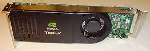
Tesla is the codename for a GPU microarchitecture developed by Nvidia as the successor to their prior microarchitectures. Tesla is Nvidia's first microarchitecture to implement unified shaders. It was used with GeForce 8 Series, GeForce 9 Series, GeForce 100 Series, GeForce 200 Series, and GeForce 300 Series of GPUs manufactured in 90 nm, 80 nm, 65 nm, and 55 nm. It also found use in the GeForce 405, and in the workstation market in the Quadro FX, Quadro x000, Quadro NVS series, and Nvidia Tesla computing modules.
Tesla replaced the old fixed-pipeline microarchitectures, represented at the time of introduction by the GeForce 7 series. It competed directly with AMD's first unified shader microarchitecture named TeraScale, a development of ATI's work on the Xbox 360 which used a similar design. Tesla was followed by Fermi. The Tesla series takes its name from pioneering electrical engineer Nikola Tesla.
Overview
Tesla is Nvidia's first microarchitecture implementing the unified shader model. The driver supports Direct3D 10 Shader Model 4.0 / OpenGL 2.1(later drivers have OpenGL 3.3 support) architecture. The design is a major shift for NVIDIA in GPU functionality and capability, the most obvious change being the move from the separate functional units (pixel shaders, vertex shaders) within previous GPUs to a homogeneous collection of universal floating point processors (called "stream processors") that can perform a more universal set of tasks.

GeForce 8's unified shader architecture consists of a number of stream processors (SPs). Unlike the vector processing approach taken with older shader units, each SP is scalar and thus can operate only on one component at a time. This makes them less complex to build while still being quite flexible and universal. Scalar shader units also have the advantage of being more efficient in a number of cases as compared to previous generation vector shader units that rely on ideal instruction mixture and ordering to reach peak throughput. The lower maximum throughput of these scalar processors is compensated for by efficiency and by running them at a high clock speed (made possible by their simplicity). GeForce 8 runs the various parts of its core at differing clock speeds (clock domains), similar to the operation of the previous GeForce 7 Series GPUs. For example, the stream processors of GeForce 8800 GTX operate at a 1.35 GHz clock rate while the rest of the chip is operating at 575 MHz.[1]
GeForce 8 performs significantly better texture filtering than its predecessors that used various optimizations and visual tricks to speed up rendering without impairing filtering quality. The GeForce 8 line correctly renders an angle-independent anisotropic filtering algorithm along with full trilinear texture filtering. G80, though not its smaller brethren, is equipped with much more texture filtering arithmetic ability than the GeForce 7 series. This allows high-quality filtering with a much smaller performance hit than previously.[1]
NVIDIA has also introduced new polygon edge anti-aliasing methods, including the ability of the GPU's ROPs to perform both Multisample anti-aliasing (MSAA) and HDR lighting at the same time, correcting various limitations of previous generations. GeForce 8 can perform MSAA with both FP16 and FP32 texture formats. GeForce 8 supports 128-bit HDR rendering, an increase from prior cards' 64-bit support. The chip's new anti-aliasing technology, called coverage sampling AA (CSAA), uses Z, color, and coverage information to determine final pixel color. This technique of color optimization allows 16X CSAA to look crisp and sharp.[2]
Performance
The claimed theoretical single-precision processing power for Tesla-based cards given in FLOPS may be hard to reach in real-world workloads.[3]
In G80/G90/GT200, each Streaming Multiprocessor (SM) contains 8 Shader Processors (SP, or Unified Shader, or CUDA Core) and 2 Special Function Units (SFU). Each SP can fulfill up to two single-precision operations per clock: 1 Multiply and 1 Add, using a single MAD instruction. Each SFU can fulfill up to four operations per clock: four MUL (Multiply) instructions. So one SM as a whole can execute 8 MADs (16 operations) and 8 MULs (8 operations) per clock, or 24 operations per clock, which is (relatively speaking) 3 times the number of SPs. Therefore, to calculate the theoretical dual-issue MAD+MUL performance in floating point operations per second [FLOPSsp+sfu, GFLOPS] of a graphics card with SP count [n] and shader frequency [f, GHz], the formula is: FLOPSsp+sfu = 3 × n × f.[4][5]
However leveraging dual-issue performance like MAD+MUL is problematic:
- Dual-issuing the MUL is not available in graphics mode on G80/G90,[6] though it was much improved in GT200.[7]
- Not all combinations of instructions like MAD+MUL can be executed in parallel on the SP and SFU, because the SFU is rather specialized as it can only handle a specific subset of instructions: 32-bit floating point multiplication, transcendental functions, interpolation for parameter blending, reciprocal, reciprocal square root, sine, cosine, etc.[8]
- The SFU could become busy for many cycles when executing these instructions, in which case it is unavailable for dual-issuing MUL instructions.[4]
For these reasons, in order to estimate the performance of real-world workloads, it may be more helpful to ignore the SFU and to assume only 1 MAD (2 operations) per SP per cycle. In this case the formula to calculate the theoretical performance in floating point operations per second becomes: FLOPSsp = 2 × n × f.
The theoretical double-precision processing power of a Tesla GPU is 1/8 of the single precision performance on GT200; there is no double precision support on G8x and G9x.[9]
Chips
Tesla 1.0
- G80
- G84
- G86
- G92
- G94
- G96
- G98
Tesla 2.0
- GT200
- GT215
- GT216
- GT218
References
- 1 2 Wasson, Scott. NVIDIA's GeForce 8800 graphics processor, Tech Report, 8 November 2007.
- ↑ Sommefeldt, Rys.NVIDIA G80: Image Quality Analysis, Beyond3D, 12 December 2006.
- ↑ "Beyond3D - NVIDIA GT200 GPU and Architecture Analysis".
- 1 2 Anand Lal Shimpi & Derek Wilson. "Derek Gets Technical: 15th Century Loom Technology Makes a Comeback - NVIDIA's 1.4 Billion Transistor GPU: GT200 Arrives as the GeForce GTX 280 & 260".
- ↑ Anand Lal Shimpi & Derek Wilson. "G80: A Mile High Overview - NVIDIA's GeForce 8800 (G80): GPUs Re-architected for DirectX 10".
- ↑ Sommefeldt, Rys. NVIDIA G80: Architecture and GPU Analysis - Page 11, Beyond3D, 8 November 2006
- ↑ "Technical Brief NVIDIA GeForce GTX 200 GPU Architectural Overview" (PDF). May 2008. p. 15. Retrieved 5 December 2015.
The individual streaming processing cores of GeForce GTX 200 GPUs can now perform near full-speed dual-issue of multiply-add operations (MADs) and MULs (3 flops/SP)
- ↑ Kanter, David (September 8, 2008). "NVIDIA's GT200: Inside a Parallel Processor". Real World Tech. p. 9.
- ↑ Smith, Ryan (17 March 2015). "The NVIDIA GeForce GTX Titan X Review". AnandTech. p. 2.
External links
| Wikimedia Commons has media related to Nvidia Tesla series. |