Stepper
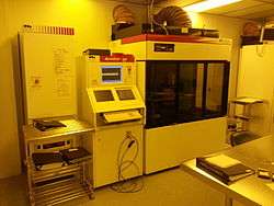
A stepper is a device used in the manufacture of integrated circuits (ICs) that is similar in operation to a slide projector or a photographic enlarger. Steppers are an essential part of the complex process, called photolithography, that creates millions of microscopic circuit elements on the surface of tiny chips of silicon. These chips form the heart of ICs such as computer processors, memory chips, and many other devices.
The stepper's role in photolithography
Elements of the circuit to be created on the IC are reproduced in a pattern of transparent and opaque areas on the surface of a quartz plate called a photomask or reticle. The stepper passes light through the reticle, forming an image of the reticle pattern. The image is focused and reduced by a lens, and projected onto the surface of a silicon wafer that is coated with a photosensitive material called photoresist.
After exposure in the stepper, the coated wafer is developed like photographic film, causing the photoresist to dissolve in certain areas according to the amount of light the areas received during exposure. These areas of photoresist and no photoresist reproduce the pattern on the reticle. The developed wafer is then exposed to acids or other chemicals. The acid etches away the silicon in the parts of the wafer that are no longer protected by the photoresist coating. The other chemicals are used to change the electrical characteristics of the silicon in the bare areas. The wafer is then cleaned, recoated with photoresist, then passed through the stepper again in a process that creates the circuit on the silicon, layer by layer. The entire process is called photolithography or photo engineering.
When the wafer is processed in the stepper, the pattern on the reticle (which may contain a number of individual chip patterns) is exposed repeatedly across the surface of the wafer in a grid. The stepper gets its name from the fact that it moves or "steps" the wafer from one shot location to another. This is accomplished by moving the wafer back and forth and left and right under the lens of the stepper. Previous generations of photolithographic equipment would expose the entire wafer, all at once; a stepper, working on a limited area, is capable of higher resolution.
As of 2008, the most detailed patterns in semiconductor device fabrication are transferred using a type of stepper called a scanner, which moves the wafer and reticle with respect to each other during the exposure, as a way of increasing the size of the exposed area and increasing the imaging performance of the lens.
Basic operation
A typical stepper has the following subassemblies: wafer loader, wafer stage, wafer alignment system, reticle loader, reticle stage, reticle alignment system, reduction lens, and illumination system. Process programs for each layer printed on the wafer are executed by a control system centering on a computer that stores the process program, reads it, and communicates with the various subassemblies of the stepper in carrying out the program's instructions. The components of the stepper are contained in a sealed chamber that is maintained at a precise temperature to prevent distortions in the printed patterns that might be caused by expansion or contraction of the wafer due to temperature variations.
The silicon wafers are coated with photoresist, and placed in a cassette or "boat" that holds a number of wafers. This is then placed in a part of the stepper called the wafer loader, usually located at the lower front of the stepper.
A robot in the wafer loader picks up one of the wafers from the cassette and loads it onto the wafer stage where it is aligned to enable another, finer alignment process that will occur later on.
The pattern of the circuitry for each chip is contained in a pattern etched in chrome on the reticle, which is a plate of transparent quartz. A typical reticle used in steppers is 6 inches square and has a usable area of 104mm by 132mm.
A variety of reticles, each appropriate for one stage in the process, are contained in a rack in the reticle loader, usually located at the upper front of the stepper. Before the wafer is exposed a reticle is loaded onto the reticle stage by a robot, where it is also very precisely aligned. Since the same reticle can be used to expose many wafers, it is loaded once before a series of wafers is exposed, and is realigned periodically.
Once the wafer and reticle are in place and aligned, the wafer stage, which is moved very precisely in the X and Y directions (front to back and left to right) by worm screws or linear motors, carries the wafer so that the first of the many patterns (or "shots") to be exposed on it is located below the lens, directly under the reticle.
Although the wafer is aligned after it is placed on the wafer stage, this alignment is not sufficient to ensure that the layer of circuitry to be printed onto the wafer exactly overlays previous layers already there. Therefore each shot is aligned using special alignment marks that are located in the pattern for each final IC chip. Once this fine alignment is completed, the shot is exposed by light from the stepper's illumination system that passes through the reticle, through a reduction lens, and on to the surface of the wafer. A process program or "recipe" determines the length of the exposure, the reticle used, as well as other factors that affect the exposure.
Each shot located in a grid pattern on the wafer and is exposed in turn as the wafer is stepped back and forth under the lens. When all shots on the wafer are exposed, the wafer is unloaded by the wafer loader robot, and another wafer takes its place on the stage. The exposed wafer is eventually moved to a developer where the photoresist on its surface is exposed to developing chemicals that wash away areas of the photoresist, based on whether or not they were exposed to the light passing through the reticle. The developed surface is then subjected to other processes of photolithography....
Major subassemblies
A typical stepper has the following subassemblies: wafer loader, wafer stage, wafer alignment system, reticle loader, reticle stage, reticle alignment system, reduction lens, and illumination system. Process programs for each layer printed on the wafer are executed by a control system centering on a computer that stores the process program, reads it, and communicates with the various subassemblies of the stepper in carrying out the program's instructions. The components of the stepper are contained in a sealed chamber that is maintained at a precise temperature to prevent distortions in the printed patterns that might be caused by expansion or contraction of the wafer due to temperature variations. The chamber also contains other systems that support the process, such as air conditioning, power supplies, control boards for the various electrical components, and others.
Illumination and the challenges of improving resolution
The greatest limitation on the ability to produce increasingly finer lines on the surface of the wafer has been the wavelength of the light used in the exposure system. As the required lines have become narrower and narrower, illumination sources producing light with progressively shorter wavelengths have been put into service in steppers and scanners.
The ability of an exposure system, such as a stepper, to resolve narrow lines is limited by the wavelength of the light used for illumination, the ability of the lens to capture light (or actually orders of diffraction) coming at increasingly wider angles (called numerical aperture or N.A.), and various improvements in the process itself. This is expressed by the following equation:

is the critical dimension, or finest line resolvable, is a coefficient expressing process-related factors, is the wavelength of the light, and is the numerical aperture. Decreasing the wavelength of the light in the illumination system increases the resolving power of the stepper.


Twenty years ago, the ultraviolet "g-line" (436 nm) of the mercury spectrum was used to create lines in the 750 nm range in steppers that employed mercury lamps as their illumination source. Several years later systems employing the "i-line" (365 nm) from mercury lamps were introduced to create lines as low as 350 nm. As the desired line widths approached and eventually became narrower than the wavelength of the light used to create them, a variety of resolution enhancement techniques were developed to make this possible, such as phase shifting reticles and various techniques for manipulating the angles of the exposure light in order to maximize the resolving power of the lens.
Eventually however, the desired line widths became narrower than what was possible using mercury lamps, and near the middle of the 2000s, the semiconductor industry moved towards steppers that employed krypton-fluoride (KrF) excimer lasers producing 248 nm light. Such systems are currently being used to produce lines in the 110 nm range. Lines as low as 32 nm are being resolved by production-capable steppers using argon-fluoride (ArF) excimer lasers that emit light with a wavelength of 193 nm. Although fluoride (F2) lasers are available that produce 157 nm light, they are not practical because of their low power and because they quickly degrade the materials used to make the lenses in the stepper.
Since practical light sources with wavelengths narrower than these lasers have not been available, manufacturers have sought to improve resolution by reducing the process coefficient . This is done by further improving techniques for manipulating the light as it passes through the illumination system and the reticle, as well as improving techniques for processing the wafer before and after exposure. Manufacturers have also introduced ever larger and more expensive lenses as a means of increasing the numerical aperture. However, these techniques are approaching their practical limit, and line widths in the 45 nm range appear to be near the best that can be achieved with conventional design.
Ultimately, other sources of illumination will have to be put to use, such as electron beams, x-rays or similar sources of electromagnetic energy with wavelengths much shorter than visible light. However, in order to delay as long as possible the vast expense and difficulty of adopting a whole new type of illumination technology, manufacturers have turned to a technique, previously used in microscopes, for increasing the numerical aperture of the lens by allowing the light to pass through water instead of air. This method, called immersion lithography, is the current cutting edge of practical production technology. It works because numerical aperture is a function of the maximum angle of light that can enter the lens and the refractive index of the medium through which the light passes. When water is employed as the medium, it greatly increases numerical aperture, since it has a refractive index of 1.44 at 193 nm, while air has an index of 1. Current production machines employing this technology are capable of resolving lines in the 32 nm range,[1] and may eventually be able to achieve lines of 30 nm.
Scanners
Modern scanners are steppers that increase the length of the area exposed in each shot (the exposure field) by moving the reticle stage and wafer stage in opposite directions to each other during the exposure. Instead of exposing the entire field at once, the exposure is made through an "exposure slit" that is as wide as the exposure field, but only a fraction of its length (such as a 9x25 mm slit for a 35x25 mm field). The image from the exposure slit is scanned across the exposure area.
 Animation showing how a scanner exposes sections of a wafer |
There are several benefits to this technique. The field can be exposed with a lesser reduction of size from the reticle to the wafer (such as 4x reduction on a scanner, compared with 5x reduction on a stepper), while allowing a field size much larger than that which can be exposed with a typical stepper. Also the optical properties of the projection lens can be optimized in the area through which the image of the projection slit passes, while optical aberrations can be ignored outside of this area, because they will not affect the exposed area on the wafer.
Successful scanning requires extremely precise synchronization between the moving reticle and wafer stages during the exposure. Accomplishing this presents many technological challenges.
See also
Stepper makers:
References
- ↑ New Product: Carl Zeiss SMT’s ‘PROVE’ handles mask pattern alignment and registration at 32nm node - Fabtech - The online information source for semiconductor professionals