Semiconductor device fabrication
| Semiconductor manufacturing processes |
|---|
 |
|
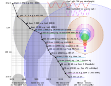
Half-nodes |
Semiconductor device fabrication is the process used to create the integrated circuits that are present in everyday electrical and electronic devices. It is a multiple-step sequence of photo lithographic and chemical processing steps during which electronic circuits are gradually created on a wafer made of pure semiconducting material. Silicon is almost always used, but various compound semiconductors are used for specialized applications.
The entire manufacturing process, from start to packaged chips ready for shipment, takes six to eight weeks and is performed in highly specialized facilities referred to as fabs.
History
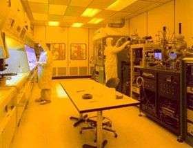
When feature widths were far greater than about 10 micrometres, purity was not the issue that it is today in device manufacturing. As devices became more integrated, cleanrooms became even cleaner. Today, the fabs are pressurized with filtered air to remove even the smallest particles, which could come to rest on the wafers and contribute to defects. The workers in a semiconductor fabrication facility are required to wear cleanroom suits to protect the devices from human contamination.
Semiconductor device manufacturing has spread from Texas and California in the 1960s to the rest of the world, including Europe, the Middle East, and Asia. It is a global business today. The leading semiconductor manufacturers typically have facilities all over the world. Intel, the world's largest manufacturer, has facilities in Europe and Asia as well as the U.S. Other top manufacturers include Taiwan Semiconductor Manufacturing Company (Taiwan), United Microelectronics Corporation (Taiwan), STMicroelectronics (Europe), Analog Devices (US), Integrated Device Technology (US), Atmel (US/Europe), Freescale Semiconductor (US), Samsung (Korea), Texas Instruments (US), IBM (US), GlobalFoundries (Germany, Singapore, US), Toshiba (Japan), NEC Electronics (Japan), Infineon (Europe, US, Asia), Renesas (Japan), Fujitsu (Japan/US), NXP Semiconductors (Europe, Asia and US), Micron Technology (US), Hynix (Korea), and SMIC (China).
Wafers
A typical wafer is made out of extremely pure silicon that is grown into mono-crystalline cylindrical ingots (boules) up to 300 mm (slightly less than 12 inches) in diameter using the Czochralski process. These ingots are then sliced into wafers about 0.75 mm thick and polished to obtain a very regular and flat surface.
Processing
In semiconductor device fabrication, the various processing steps fall into four general categories: deposition, removal, patterning, and modification of electrical properties.
- Deposition is any process that grows, coats, or otherwise transfers a material onto the wafer. Available technologies include physical vapor deposition (PVD), chemical vapor deposition (CVD), electrochemical deposition (ECD), molecular beam epitaxy (MBE) and more recently, atomic layer deposition (ALD) among others.
- Removal is any process that removes material from the wafer; examples include etch processes (either wet or dry) and chemical-mechanical planarization (CMP).
- Patterning is the shaping or altering of deposited materials, and is generally referred to as lithography. For example, in conventional lithography, the wafer is coated with a chemical called a photoresist; then, a machine called a stepper focuses, aligns, and moves a mask, exposing select portions of the wafer below to short wavelength light; the exposed regions are washed away by a developer solution. After etching or other processing, the remaining photoresist is removed by plasma ashing.
- Modification of electrical properties has historically entailed doping transistor sources and drains (originally by diffusion furnaces and later by ion implantation). These doping processes are followed by furnace annealing or, in advanced devices, by rapid thermal annealing (RTA); annealing serves to activate the implanted dopants. Modification of electrical properties now also extends to the reduction of a material's dielectric constant in low-k insulators via exposure to ultraviolet light in UV processing (UVP).
Modern chips have up to eleven metal levels produced in over 300 sequenced processing steps.
Front-end-of-line (FEOL) processing
FEOL processing refers to the formation of the transistors directly in the silicon. The raw wafer is engineered by the growth of an ultrapure, virtually defect-free silicon layer through epitaxy. In the most advanced logic devices, prior to the silicon epitaxy step, tricks are performed to improve the performance of the transistors to be built. One method involves introducing a straining step wherein a silicon variant such as silicon-germanium (SiGe) is deposited. Once the epitaxial silicon is deposited, the crystal lattice becomes stretched somewhat, resulting in improved electronic mobility. Another method, called silicon on insulator technology involves the insertion of an insulating layer between the raw silicon wafer and the thin layer of subsequent silicon epitaxy. This method results in the creation of transistors with reduced parasitic effects.
Gate oxide and implants
Front-end surface engineering is followed by growth of the gate dielectric (traditionally silicon dioxide), patterning of the gate, patterning of the source and drain regions, and subsequent implantation or diffusion of dopants to obtain the desired complementary electrical properties. In dynamic random-access memory (DRAM) devices, storage capacitors are also fabricated at this time, typically stacked above the access transistor (the now defunct DRAM manufacturer Qimonda implemented these capacitors with trenches etched deep into the silicon surface).
Back-end-of-line (BEOL) processing
Metal layers
Once the various semiconductor devices have been created, they must be interconnected to form the desired electrical circuits. This occurs in a series of wafer processing steps collectively referred to as BEOL (not to be confused with back end of chip fabrication, which refers to the packaging and testing stages). BEOL processing involves creating metal interconnecting wires that are isolated by dielectric layers. The insulating material has traditionally been a form of SiO2 or a silicate glass, but recently new low dielectric constant materials are being used (such as silicon oxycarbide), typically providing dielectric constants around 2.7 (compared to 3.9 for SiO2), although materials with constants as low as 2.2 are being offered to chipmakers.
Interconnect
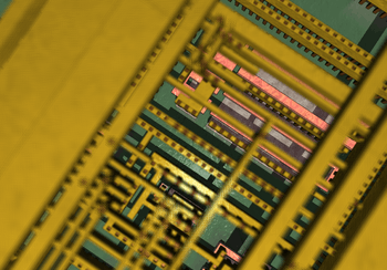
Historically, the metal wires have been composed of aluminum. In this approach to wiring (often called subtractive aluminum), blanket films of aluminum are deposited first, patterned, and then etched, leaving isolated wires. Dielectric material is then deposited over the exposed wires. The various metal layers are interconnected by etching holes (called "vias") in the insulating material and then depositing tungsten in them with a CVD technique; this approach is still used in the fabrication of many memory chips such as dynamic random-access memory (DRAM), because the number of interconnect levels is small (currently no more than four).
More recently, as the number of interconnect levels for logic has substantially increased due to the large number of transistors that are now interconnected in a modern microprocessor, the timing delay in the wiring has become so significant as to prompt a change in wiring material (from aluminum to copper layer) and a change in dielectric material (from silicon dioxides to newer low-K insulators). This performance enhancement also comes at a reduced cost via damascene processing, which eliminates processing steps. As the number of interconnect levels increases, planarization of the previous layers is required to ensure a flat surface prior to subsequent lithography. Without it, the levels would become increasingly crooked, extending outside the depth of focus of available lithography, and thus interfering with the ability to pattern. CMP (chemical-mechanical planarization) is the primary processing method to achieve such planarization, although dry etch back is still sometimes employed when the number of interconnect levels is no more than three.
Wafer test
The highly serialized nature of wafer processing has increased the demand for metrology in between the various processing steps. For example, thin film metrology based on ellipsometry or reflectometry is used to tightly control the thickness of gate oxide, as well as the thickness, refractive index and extinction coefficient of photoresist and other coatings. Wafer test metrology equipment is used to verify that the wafers haven't been damaged by previous processing steps up until testing; if too many dies on one wafer have failed, the entire wafer is scrapped to avoid the costs of further processing. Virtual metrology has been used to predict wafer properties based on statistical methods without performing the physical measurement itself.[1]
Device test
Once the front-end process has been completed, the semiconductor devices are subjected to a variety of electrical tests to determine if they function properly. The proportion of devices on the wafer found to perform properly is referred to as the yield. Manufacturers are typically secretive about their yields, but it can be as low as 30%. Process variation is one among many reasons for low yield.[2]
The fab tests the chips on the wafer with an electronic tester that presses tiny probes against the chip. The machine marks each bad chip with a drop of dye. Currently, electronic dye marking is possible if wafer test data is logged into a central computer database and chips are "binned" (i.e. sorted into virtual bins) according to the predetermined test limits. The resulting binning data can be graphed, or logged, on a wafer map to trace manufacturing defects and mark bad chips. This map can also be used during wafer assembly and packaging.
Chips are also tested again after packaging, as the bond wires may be missing, or analog performance may be altered by the package. This is referred to as the "final test".
Usually, the fab charges for testing time, with prices in the order of cents per second. Testing times vary from a few milliseconds to a couple of seconds, and the test software is optimized for reduced testing time. Multiple chip (multi-site) testing is also possible, because many testers have the resources to perform most or all of the tests in parallel.
Chips are often designed with "testability features" such as scan chains or a "built-in self-test" to speed testing, and reduce testing costs. In certain designs that use specialized analog fab processes, wafers are also laser-trimmed during the testing, in order to achieve tightly-distributed resistance values as specified by the design.
Good designs try to test and statistically manage corners (extremes of silicon behavior caused by a high operating temperature combined with the extremes of fab processing steps). Most designs cope with at least 64 corners.
Die preparation
Once tested, a wafer is typically reduced in thickness before the wafer is scored and then broken into individual dice, a process known as wafer dicing. Only the good, unmarked chips are packaged.
Packaging
Plastic or ceramic packaging involves mounting the die, connecting the die pads to the pins on the package, and sealing the die. Tiny wires are used to connect the pads to the pins. In the old days, wires were attached by hand, but now specialized machines perform the task. Traditionally, these wires have been composed of gold, leading to a lead frame (pronounced "leed frame") of solder-plated copper; lead is poisonous, so lead-free "lead frames" are now mandated by RoHS.
Chip scale package (CSP) is another packaging technology. A plastic dual in-line package, like most packages, is many times larger than the actual die hidden inside, whereas CSP chips are nearly the size of the die; a CSP can be constructed for each die before the wafer is diced.
The packaged chips are retested to ensure that they were not damaged during packaging and that the die-to-pin interconnect operation was performed correctly. A laser then etches the chip's name and numbers on the package.
List of steps
This is a list of processing techniques that are employed numerous times throughout the construction of a modern electronic device; this list does not necessarily imply a specific order.
- Wafer processing
- Wet cleans
- Cleaning by solvents such as acetone, trichloroethylene
- Piranha solution
- RCA clean
- Photolithography
- Ion implantation (in which dopants are embedded in the wafer creating regions of increased (or decreased) conductivity)
- Dry etching
- Wet etching
- Plasma ashing
- Thermal treatments
- Chemical vapor deposition (CVD)
- Physical vapor deposition (PVD)
- Molecular beam epitaxy (MBE)
- Electrochemical deposition (ECD). See Electroplating
- Chemical-mechanical planarization (CMP)
- Wafer testing (where the electrical performance is verified)
- Wafer backgrinding (to reduce the thickness of the wafer so the resulting chip can be put into a thin device like a smartcard or PCMCIA card.)
- Wet cleans
- Die preparation
- Wafer mounting
- Die cutting
- IC packaging
- Die attachment
- IC bonding
- IC encapsulation
- Baking
- Plating
- Lasermarking
- Trim and form
- IC testing
Hazardous materials
Many toxic materials are used in the fabrication process.[3] These include:
- poisonous elemental dopants, such as arsenic, antimony, and phosphorus.
- poisonous compounds, such as arsine, phosphine, and silane.
- highly reactive liquids, such as hydrogen peroxide, fuming nitric acid, sulfuric acid, and hydrofluoric acid.
It is vital that workers should not be directly exposed to these dangerous substances. The high degree of automation common in the IC fabrication industry helps to reduce the risks of exposure. Most fabrication facilities employ exhaust management systems, such as wet scrubbers, combustors, heated absorber cartridges, etc., to control the risk to workers and to the environment.
See also
- List of semiconductor scale examples
- Electronic design automation (EDA)
- Information technology (IT)
- International Technology Roadmap for Semiconductors
- Semiconductor consolidation
- List of semiconductor fabrication plants
- Microfabrication
- Semiconductor Equipment and Materials International (SEMI) — the semiconductor industry trade association
- SEMI font for labels on wafers
- Design For Test
- On-board diagnostics
- Built-In Test Equipment
- Hardware description language (HDL)
- VHDL / Verilog, hardware description language
- Computer simulation
- Etch pit density
- Built-in self-test
- Passivation
- Hydrogen-terminated silicon surface
- planar process
- Surface-mount technology (SMT)
- Health hazards in semiconductor manufacturing occupations
References
- ↑ Neurotechnology Group, Berlin Institute of Technology, IEEE Xplore Digital Library. “Regression Methods for Virtual Metrology of Layer Thickness in Chemical Vapor Deposition.” January 17, 2014. Retrieved November 9, 2015.
- ↑ "A Survey Of Architectural Techniques for Managing Process Variation", ACM Computing Surveys, 2015
- ↑ CNET. “Why tech pollution's going global.” April 25, 2002. Retrieved November 9, 2015.
Further reading
- Kaeslin, Hubert (2008), Digital Integrated Circuit Design, from VLSI Architectures to CMOS Fabrication, Cambridge University Press, section 14.2.
External links
- Semiconductor glossary
- Wafer heating
- Designing a Heated Chuck for Semiconductor Processing Equipment