Scanning electron microscope
A scanning electron microscope (SEM) is a type of electron microscope that produces images of a sample by scanning it with a focused beam of electrons. The electrons interact with atoms in the sample, producing various signals that contain information about the sample's surface topography and composition. The electron beam is generally scanned in a raster scan pattern, and the beam's position is combined with the detected signal to produce an image. SEM can achieve resolution better than 1 nanometer. Specimens can be observed in high vacuum, in low vacuum, in wet conditions (in environmental SEM), and at a wide range of cryogenic or elevated temperatures.
The most common SEM mode is detection of secondary electrons emitted by atoms excited by the electron beam. The number of secondary electrons that can be detected depends, among other things, on specimen topography. By scanning the sample and collecting the secondary electrons that are emitted using a special detector, an image displaying the topography of the surface is created.
History
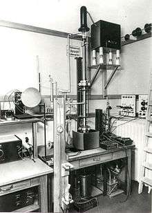
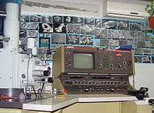
An account of the early history of SEM has been presented by McMullan.[1][2] Although Max Knoll produced a photo with a 50 mm object-field-width showing channeling contrast by the use of an electron beam scanner,[3] it was Manfred von Ardenne who in 1937 invented[4] a true microscope with high magnification by scanning a very small raster with a demagnified and finely focused electron beam. Ardenne applied the scanning principle not only to achieve magnification but also to purposefully eliminate the chromatic aberration otherwise inherent in the electron microscope. He further discussed the various detection modes, possibilities and theory of SEM,[5] together with the construction of the first high magnification SEM.[6] Further work was reported by Zworykin's group,[7] followed by the Cambridge groups in the 1950s and early 1960s[8][9][10][11] headed by Charles Oatley, all of which finally led to the marketing of the first commercial instrument by Cambridge Scientific Instrument Company as the "Stereoscan" in 1965, which was delivered to DuPont.
Principles and capacities
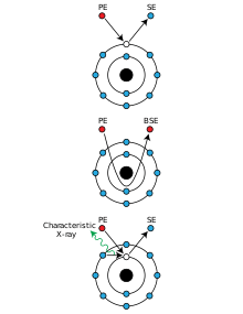
The types of signals produced by an SEM include secondary electrons (SE), reflected or back-scattered electrons (BSE), photons of characteristic X-rays and light (cathodoluminescence) (CL), absorbed current (specimen current) and transmitted electrons. Secondary electron detectors are standard equipment in all SEMs, but it is rare that a single machine would have detectors for all other possible signals.
The signals result from interactions of the electron beam with atoms at various depths within the sample. In the most common or standard detection mode, secondary electron imaging or SEI, the secondary electrons are emitted from very close to the specimen surface. Consequently, SEM can produce very high-resolution images of a sample surface, revealing details less than 1 nm in size. Back-scattered electrons (BSE) are beam electrons that are reflected from the sample by elastic scattering. They emerge from deeper locations within the specimen and consequently the resolution of BSE images is generally poorer than SE images. However, BSE are often used in analytical SEM along with the spectra made from the characteristic X-rays, because the intensity of the BSE signal is strongly related to the atomic number (Z) of the specimen. BSE images can provide information about the distribution of different elements in the sample. For the same reason, BSE imaging can image colloidal gold immuno-labels of 5 or 10 nm diameter, which would otherwise be difficult or impossible to detect in secondary electron images in biological specimens. Characteristic X-rays are emitted when the electron beam removes an inner shell electron from the sample, causing a higher-energy electron to fill the shell and release energy. These characteristic X-rays are used to identify the composition and measure the abundance of elements in the sample.
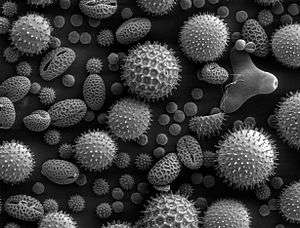
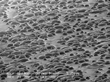
Due to the very narrow electron beam, SEM micrographs have a large depth of field yielding a characteristic three-dimensional appearance useful for understanding the surface structure of a sample. This is exemplified by the micrograph of pollen shown above. A wide range of magnifications is possible, from about 10 times (about equivalent to that of a powerful hand-lens) to more than 500,000 times, about 250 times the magnification limit of the best light microscopes.
Sample preparation
Samples for SEM can be solid, bulk specimens of any size that will fit within the specimen chamber. Samples are generally mounted rigidly on a specimen holder called a specimen stub using a conductive adhesive, but mechanical clamping is a possible alternative. Several models of SEM can examine any part of a 6-inch (15 cm) semiconductor wafer, and some can tilt an object of that size to 45° and provide continuous 360° rotation.
Nonconductive specimens tend to charge when scanned by the electron beam, and especially in secondary electron imaging mode, this causes scanning faults and other image artifacts. For conventional imaging in the SEM, specimens must be electrically conductive, at least at the surface, and electrically grounded to prevent the accumulation of electrostatic charge. Metal objects require little special preparation for SEM except for cleaning and mounting on a specimen stub. Non-conducting materials are usually coated with an ultrathin coating of electrically conducting material, deposited on the sample either by low-vacuum sputter coating or by high-vacuum evaporation. Conductive materials in current use for specimen coating include gold, gold/palladium alloy, platinum, osmium,[12] iridium, tungsten, chromium, and graphite. Coating with heavy metals may increase signal/noise ratio for samples of low atomic number (Z). The improvement arises because secondary electron emission for high-Z materials is enhanced.
An alternative to coating for some biological samples is to increase the bulk conductivity of the material by impregnation with osmium using variants of the OTO staining method (O-osmium tetroxide, T-thiocarbohydrazide, O-osmium).[13][14]
Nonconducting specimens may be imaged without coating using an environmental SEM (ESEM) or low-voltage mode of SEM operation.[15] In ESEM instruments the specimen is placed in a relatively high-pressure chamber and the electron optical column is differentially pumped to keep vacuum adequately low at the electron gun. The high-pressure region around the sample in the ESEM neutralizes charge and provides an amplification of the secondary electron signal. Low-voltage SEM is typically conducted in an FEG-SEM because field emission guns (FEG) are capable of producing high primary electron brightness and small spot size even at low accelerating potentials. To prevent charging of non-conductive specimens, operating conditions must be adjusted such that the incoming beam current is equal to sum of outcoming secondary and backscattered electrons currents a condition that is more often met at accelerating voltages of 0.3–4 kV.
Synthetic replicas can be made to avoid the use of original samples when they are not suitable or available for SEM examination due to methodological obstacles or legal issues. This technique is achieved in two steps: (1) a mold of the original surface is made using a silicone-based dental elastomer, and (2) a replica of the original surface is obtained by pouring a synthetic resin into the mold.[16]
Embedding in a resin with further polishing to a mirror-like finish can be used for both biological and materials specimens when imaging in backscattered electrons or when doing quantitative X-ray microanalysis.
The main preparation techniques are not required in the environmental SEM outlined below, but some biological specimens can benefit from fixation.
Biological samples
For SEM, a specimen is normally required to be completely dry, since the specimen chamber is at high vacuum. Hard, dry materials such as wood, bone, feathers, dried insects, or shells (including egg shells[17]) can be examined with little further treatment, but living cells and tissues and whole, soft-bodied organisms usually require chemical fixation to preserve and stabilize their structure.
Fixation is usually performed by incubation in a solution of a buffered chemical fixative, such as glutaraldehyde, sometimes in combination with formaldehyde[18][19][20] and other fixatives,[21] and optionally followed by postfixation with osmium tetroxide.[18] The fixed tissue is then dehydrated. Because air-drying causes collapse and shrinkage, this is commonly achieved by replacement of water in the cells with organic solvents such as ethanol or acetone, and replacement of these solvents in turn with a transitional fluid such as liquid carbon dioxide by critical point drying. The carbon dioxide is finally removed while in a supercritical state, so that no gas–liquid interface is present within the sample during drying.
The dry specimen is usually mounted on a specimen stub using an adhesive such as epoxy resin or electrically conductive double-sided adhesive tape, and sputter-coated with gold or gold/palladium alloy before examination in the microscope. Other samples may require sectioning (with a microtome) and staining.
If the SEM is equipped with a cold stage for cryo microscopy, cryofixation may be used and low-temperature scanning electron microscopy performed on the cryogenically fixed specimens.[18] Cryo-fixed specimens may be cryo-fractured under vacuum in a special apparatus to reveal internal structure, sputter-coated, and transferred onto the SEM cryo-stage while still frozen.[22] Low-temperature scanning electron microscopy (LT-SEM) is also applicable to the imaging of temperature-sensitive materials such as ice[23][24] and fats.[25]
Freeze-fracturing, freeze-etch or freeze-and-break is a preparation method particularly useful for examining lipid membranes and their incorporated proteins in "face on" view. The preparation method reveals the proteins embedded in the lipid bilayer.
Materials
Back-scattered electron imaging, quantitative X-ray analysis, and X-ray mapping of specimens often requires grinding and polishing the surfaces to an ultra smooth surface. Specimens that undergo WDS or EDS analysis are often carbon-coated. In general, metals are not coated prior to imaging in the SEM because they are conductive and provide their own pathway to ground.
Fractography is the study of fractured surfaces that can be done on a light microscope or, commonly, on an SEM. The fractured surface is cut to a suitable size, cleaned of any organic residues, and mounted on a specimen holder for viewing in the SEM.
Integrated circuits may be cut with a focused ion beam (FIB) or other ion beam milling instrument for viewing in the SEM. The SEM in the first case may be incorporated into the FIB.
Metals, geological specimens, and integrated circuits all may also be chemically polished for viewing in the SEM.
Special high-resolution coating techniques are required for high-magnification imaging of inorganic thin films.
Scanning process and image formation
.svg.png)
In a typical SEM, an electron beam is thermionically emitted from an electron gun fitted with a tungsten filament cathode. Tungsten is normally used in thermionic electron guns because it has the highest melting point and lowest vapor pressure of all metals, thereby allowing it to be electrically heated for electron emission, and because of its low cost. Other types of electron emitters include lanthanum hexaboride (LaB
6) cathodes, which can be used in a standard tungsten filament SEM if the vacuum system is upgraded or field emission guns (FEG), which may be of the cold-cathode type using tungsten single crystal emitters or the thermally assisted Schottky type, that use emitters of zirconium oxide.
The electron beam, which typically has an energy ranging from 0.2 keV to 40 keV, is focused by one or two condenser lenses to a spot about 0.4 nm to 5 nm in diameter. The beam passes through pairs of scanning coils or pairs of deflector plates in the electron column, typically in the final lens, which deflect the beam in the x and y axes so that it scans in a raster fashion over a rectangular area of the sample surface.
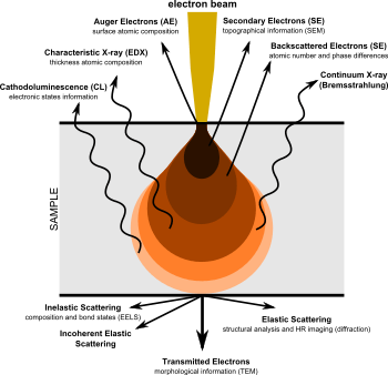
When the primary electron beam interacts with the sample, the electrons lose energy by repeated random scattering and absorption within a teardrop-shaped volume of the specimen known as the interaction volume, which extends from less than 100 nm to approximately 5 µm into the surface. The size of the interaction volume depends on the electron's landing energy, the atomic number of the specimen and the specimen's density. The energy exchange between the electron beam and the sample results in the reflection of high-energy electrons by elastic scattering, emission of secondary electrons by inelastic scattering and the emission of electromagnetic radiation, each of which can be detected by specialized detectors. The beam current absorbed by the specimen can also be detected and used to create images of the distribution of specimen current. Electronic amplifiers of various types are used to amplify the signals, which are displayed as variations in brightness on a computer monitor (or, for vintage models, on a cathode ray tube). Each pixel of computer video memory is synchronized with the position of the beam on the specimen in the microscope, and the resulting image is therefore a distribution map of the intensity of the signal being emitted from the scanned area of the specimen. In older microscopes images may be captured by photography from a high-resolution cathode ray tube, but in modern machines they are digitised and saved as digital images.
Magnification
Magnification in an SEM can be controlled over a range of about 6 orders of magnitude from about 10 to 500,000 times. Unlike optical and transmission electron microscopes, image magnification in an SEM is not a function of the power of the objective lens. SEMs may have condenser and objective lenses, but their function is to focus the beam to a spot, and not to image the specimen. Provided the electron gun can generate a beam with sufficiently small diameter, an SEM could in principle work entirely without condenser or objective lenses, although it might not be very versatile or achieve very high resolution. In an SEM, as in scanning probe microscopy, magnification results from the ratio of the dimensions of the raster on the specimen and the raster on the display device. Assuming that the display screen has a fixed size, higher magnification results from reducing the size of the raster on the specimen, and vice versa. Magnification is therefore controlled by the current supplied to the x, y scanning coils, or the voltage supplied to the x, y deflector plates, and not by objective lens power.
Detection of secondary electrons
The most common imaging mode collects low-energy (<50 eV) secondary electrons that are ejected from the k-shell of the specimen atoms by inelastic scattering interactions with beam electrons. Due to their low energy, these electrons originate within a few nanometers from the sample surface.[26] The electrons are detected by an Everhart-Thornley detector,[27] which is a type of scintillator-photomultiplier system. The secondary electrons are first collected by attracting them towards an electrically biased grid at about +400 V, and then further accelerated towards a phosphor or scintillator positively biased to about +2,000 V. The accelerated secondary electrons are now sufficiently energetic to cause the scintillator to emit flashes of light (cathodoluminescence), which are conducted to a photomultiplier outside the SEM column via a light pipe and a window in the wall of the specimen chamber. The amplified electrical signal output by the photomultiplier is displayed as a two-dimensional intensity distribution that can be viewed and photographed on an analogue video display, or subjected to analog-to-digital conversion and displayed and saved as a digital image. This process relies on a raster-scanned primary beam. The brightness of the signal depends on the number of secondary electrons reaching the detector. If the beam enters the sample perpendicular to the surface, then the activated region is uniform about the axis of the beam and a certain number of electrons "escape" from within the sample. As the angle of incidence increases, the interaction volume increases and the "escape" distance of one side of the beam decreases, resulting in more secondary electrons being emitted from the sample. Thus steep surfaces and edges tend to be brighter than flat surfaces, which results in images with a well-defined, three-dimensional appearance. Using the signal of secondary electrons image resolution less than 0.5 nm is possible.
Detection of backscattered electrons
Top: backscattered electron analysis – composition
Bottom: secondary electron analysis – topography
Backscattered electrons (BSE) consist of high-energy electrons originating in the electron beam, that are reflected or back-scattered out of the specimen interaction volume by elastic scattering interactions with specimen atoms. Since heavy elements (high atomic number) backscatter electrons more strongly than light elements (low atomic number), and thus appear brighter in the image, BSE are used to detect contrast between areas with different chemical compositions.[26] The Everhart-Thornley detector, which is normally positioned to one side of the specimen, is inefficient for the detection of backscattered electrons because few such electrons are emitted in the solid angle subtended by the detector, and because the positively biased detection grid has little ability to attract the higher energy BSE. Dedicated backscattered electron detectors are positioned above the sample in a "doughnut" type arrangement, concentric with the electron beam, maximizing the solid angle of collection. BSE detectors are usually either of scintillator or of semiconductor types. When all parts of the detector are used to collect electrons symmetrically about the beam, atomic number contrast is produced. However, strong topographic contrast is produced by collecting back-scattered electrons from one side above the specimen using an asymmetrical, directional BSE detector; the resulting contrast appears as illumination of the topography from that side. Semiconductor detectors can be made in radial segments that can be switched in or out to control the type of contrast produced and its directionality.
Backscattered electrons can also be used to form an electron backscatter diffraction (EBSD) image that can be used to determine the crystallographic structure of the specimen.
Beam-injection analysis of semiconductors
The nature of the SEM's probe, energetic electrons, makes it uniquely suited to examining the optical and electronic properties of semiconductor materials. The high-energy electrons from the SEM beam will inject charge carriers into the semiconductor. Thus, beam electrons lose energy by promoting electrons from the valence band into the conduction band, leaving behind holes.
In a direct bandgap material, recombination of these electron-hole pairs will result in cathodoluminescence; if the sample contains an internal electric field, such as is present at a p-n junction, the SEM beam injection of carriers will cause electron beam induced current (EBIC) to flow. Cathodoluminescence and EBIC are referred to as "beam-injection" techniques, and are very powerful probes of the optoelectronic behavior of semiconductors, in particular for studying nanoscale features and defects.
Cathodoluminescence
Cathodoluminescence, the emission of light when atoms excited by high-energy electrons return to their ground state, is analogous to UV-induced fluorescence, and some materials such as zinc sulfide and some fluorescent dyes, exhibit both phenomena. Over the last decades, cathodoluminescence was most commonly experienced as the light emission from the inner surface of the cathode ray tube in television sets and computer CRT monitors. In the SEM, CL detectors either collect all light emitted by the specimen or can analyse the wavelengths emitted by the specimen and display an emission spectrum or an image of the distribution of cathodoluminescence emitted by the specimen in real color.
X-ray microanalysis
Characteristic X-rays that are produced by the interaction of electrons with the sample may also be detected in an SEM equipped for energy-dispersive X-ray spectroscopy or wavelength dispersive X-ray spectroscopy. Analysis of the x-ray signals may be used to map the distribution and estimate the abundance of elements in the sample.
Resolution of the SEM
SEM is not a camera and the detector is not continuously image-forming like a CCD array or film. Unlike in an optical system, the resolution is not limited by the diffraction limit, fineness of lenses or mirrors or detector array resolution. The focusing optics can be large and coarse, and the SE detector is fist-sized and simply detects current. Instead, the spatial resolution of the SEM depends on the size of the electron spot, which in turn depends on both the wavelength of the electrons and the electron-optical system that produces the scanning beam. The resolution is also limited by the size of the interaction volume, the volume of specimen material that interacts with the electron beam. The spot size and the interaction volume are both large compared to the distances between atoms, so the resolution of the SEM is not high enough to image individual atoms, as is possible transmission electron microscope (TEM). The SEM has compensating advantages, though, including the ability to image a comparatively large area of the specimen; the ability to image bulk materials (not just thin films or foils); and the variety of analytical modes available for measuring the composition and properties of the specimen. Depending on the instrument, the resolution can fall somewhere between less than 1 nm and 20 nm. As of 2009, The world's highest resolution conventional (<30 kV) SEM can reach a point resolution of 0.4 nm using a secondary electron detector.[28]
Environmental SEM
Conventional SEM requires samples to be imaged under vacuum, because a gas atmosphere rapidly spreads and attenuates electron beams. As a consequence, samples that produce a significant amount of vapour, e.g. wet biological samples or oil-bearing rock, must be either dried or cryogenically frozen. Processes involving phase transitions, such as the drying of adhesives or melting of alloys, liquid transport, chemical reactions, and solid-air-gas systems, in general cannot be observed. Some observations of living insects have been possible however.
The first commercial development of the ESEM in the late 1980s [29][30] allowed samples to be observed in low-pressure gaseous environments (e.g. 1–50 Torr or 0.1–6.7 kPa) and high relative humidity (up to 100%). This was made possible by the development of a secondary-electron detector [31][32] capable of operating in the presence of water vapour and by the use of pressure-limiting apertures with differential pumping in the path of the electron beam to separate the vacuum region (around the gun and lenses) from the sample chamber.
The first commercial ESEMs were produced by the ElectroScan Corporation in USA in 1988. ElectroScan was taken over by Philips (who later sold their electron-optics division to FEI Company) in 1996.[33]
ESEM is especially useful for non-metallic and biological materials because coating with carbon or gold is unnecessary. Uncoated Plastics and Elastomers can be routinely examined, as can uncoated biological samples. Coating can be difficult to reverse, may conceal small features on the surface of the sample and may reduce the value of the results obtained. X-ray analysis is difficult with a coating of a heavy metal, so carbon coatings are routinely used in conventional SEMs, but ESEM makes it possible to perform X-ray microanalysis on uncoated non-conductive specimens; however some specific for ESEM artifacts are introduced in X-ray analysis. ESEM may be the preferred for electron microscopy of unique samples from criminal or civil actions, where forensic analysis may need to be repeated by several different experts.
Transmission SEM
The SEM can also be used in transmission mode by simply incorporating an appropriate detector below a thin specimen section .[34] Both bright and dark field imaging has been reported in the generally low accelerating beam voltage range used in SEM, which increases the contrast of unstained biological specimens at high magnifications with a field emission electron gun. This mode of operation has been abbreviated by the acronym tSEM.
Color in SEM
Electron microscopes do not naturally produce color images, as a SEM produces a single value per pixel; this value corresponds to the number of electrons received by the detector during a small period of time of the scanning when the beam is targeted to the (x,y) pixel position.
This single number is usually represented, for each pixel, by a grey level, forming a "black-and-white" image.[35] However, several ways have been used to get color electron microscopy images.[36]
False color using a single detector
- On compositional images of flat surfaces (typically BSE):
The easiest way to get color is to associate to this single number an arbitrary color, using a color look-up table (i.e. each grey level is replaced by a chosen color). This method is known as false color. On a BSE image, false color may be performed to better distinguish the various phases of the sample.
- On textured-surface images:
As an alternative to simply replacing each grey level by a color, a sample observed by an oblique beam allows to create an approximative topography image (see further section "Photometric 3D rendering from a single SEM image"). Such topography can then be processed by 3D-rendering algorithms for a more natural rendering of the surface texture
 Surface of a kidney stone
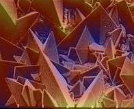 The same after re-processing of the color from the estimated topography
 SEM image of a diagenetically altered discoaster
 The same image after similar colorization
SEM image coloring
Very often, published SEM images are artificially colored. This may be done for aesthetic effect, to clarify structure or to add a realistic appearance to the sample[37] and generally does not add information about the specimen.[38]
Coloring may be performed manually with photo-editing software, or semi-automatically with dedicated software using feature-detection or object-oriented segmentation.[39]
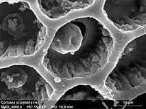 SEM image of Cobaea scandens pollen
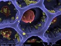 The same after semi-automatic coloring. Arbitrary colors help identifying the various elements of the structure
 Colored SEM image of Tradescantia pollen and stamens
Color built using multiple electron detectors
In some configurations more information is gathered per pixel, often by the use of multiple detectors.[40]
As a common example, secondary electron and backscattered electron detectors are superimposed and a color is assigned to each of the images captured by each detector,[41][42] with an end result of a combined color image where colors are related to the density of the components. This method is known as density-dependent color SEM (DDC-SEM). Micrographs produced by DDC-SEM retain topographical information, which is better captured by the secondary electrons detector and combine it to the information about density, obtained by the backscattered electron detector.[43][44]
 DDC-SEM of calcified particle in cardiac tissue - Signal 1 : SE
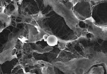 Signal 2 : BSE
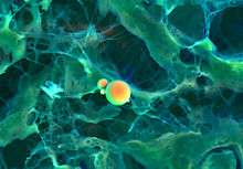 Colorized image obtained from the two previous. Density-dependent color scanning electron micrograph SEM (DDC-SEM) of cardiovascular calcification, showing in orange a calcium phosphate spherical particle (denser material) and, in green, the extracellular matrix (less dense material)
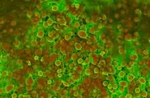 Same work with a larger view, part of a study on human cardiovascular tissue calcification
Analytical signals based on generated photons
Measurement of the energy of photons emitted from the specimen is a common method to get analytical capabilities. Examples are the Energy-dispersive X-ray spectroscopy (EDS) detectors used in elemental analysis and Cathodoluminescence microscope (CL) systems that analyse the intensity and spectrum of electron-induced luminescence in (for example) geological specimens. In SEM systems using these detectors it is common to color code these extra signals and superimpose them in a single color image, so that differences in the distribution of the various components of the specimen can be seen clearly and compared. Optionally, the standard secondary electron image can be merged with the one or more compositional channels, so that the specimen's structure and composition can be compared. Such images can be made while maintaining the full integrity of the original signal data, which is not modified in any way.
3D in SEM
SEMs do not naturally provide 3D images contrary to SPMs. However 3D data can be obtained using an SEM with different methods as follows.
3D SEM reconstruction from a stereo pair
- photogrammetry (2 or 3 images from tilted specimen)
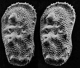 An SEM stereo pair of microfossils of less than 1 mm in size (Ostracoda) produced by tilting along the longitudinal axis.
.gif) From this pair of SEM images, the third dimension has been reconstructed by photogrammetry (using MountainsMap software) ; then a series of 3D representations with different angles have been made and assembled into a GIF file to produce this animation.
From this pair of SEM images, the third dimension has been reconstructed by photogrammetry (using MountainsMap software) ; then a series of 3D representations with different angles have been made and assembled into a GIF file to produce this animation.
Photometric 3D SEM reconstruction from a four-quadrant detector "shape from shading"
This method typically uses a four-quadrant BSE detector. The microscope produces four images of the same specimen at the same time, so no tilt is required. The method gives metrological 3D dimensions as far as the slope of the specimen remains reasonable. As it works by integration of the slope, vertical slopes and overhangs are ignored ; for instance, if an entire sphere lies on a flat, only the main part of the upper hemisphere is seen emerging above the flat, resulting in wrong altitude of the sphere apex.
Photometric 3D rendering from a single SEM image
This method requires an SEM image obtained in oblique low angle lighting. The grey-level is then interpreted as the slope, and the slope integrated to restore the specimen topography. This method is interesting for visual enhancement and the detection of the shape and position of objects ; however the vertical heights cannot usually be calibrated, contrary to other methods such as photogrammetry.
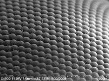 SEM image of a house fly compound eye surface at 450× magnification.
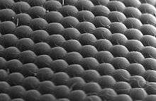 Detail of the previous image.
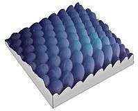 SEM 3D reconstruction from the previous using shape from shading algorithms.
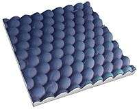 Same as the previous, but with lighting homogenized before applying the shape from shading algorithms
Other types of 3D SEM reconstruction
- inverse reconstruction using electron-material interactive models[45][46]
- vertical stacks of SEM micrographs plus image-processing software[47]
- Multi-Resolution reconstruction using single 2D File: High-quality 3D imaging may be an ultimate solution for revealing the complexities of any porous media, but acquiring them is costly and time consuming. High-quality 2D SEM images, on the other hand, are widely available. Recently, a novel three-step, multiscale, multiresolution reconstruction method is presented that directly uses 2D images in order to develop 3D models. This method, based on a Shannon Entropy and conditional simulation, can be used for most of the available stationary materials and can build various stochastic 3D models just using a few thin sections.[48]
Applications of 3D SEM
Possible applications are roughness measurement, measurement of fractal dimension, examining fracture surface of metals, characterization of materials, corrosion measurement, and dimensional measurements at the nano scale (step height, volume, angle, flatness, bearing ratio, coplanarity, etc.).
Gallery of SEM images
The following are examples of images taken using an SEM.
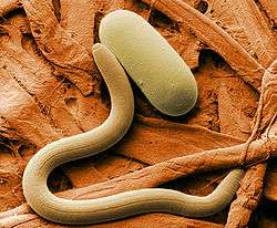 Colored SEM image of soybean cyst nematode and egg. The artificial coloring makes the image easier for non-specialists to view and understand the structures and surfaces revealed in micrographs.
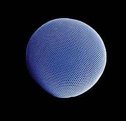 Compound eye of Antarctic krill Euphausia superba. Arthropod eyes are a common subject in SEM micrographs due to the depth of focus that an SEM image can capture. Colored picture.
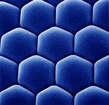 Ommatidia of Antarctic krill eye, a higher magnification of the krill's eye. SEMs cover a range from light microscopy up to the magnifications available with a TEM. Colored picture.
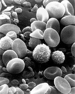 SEM image of normal circulating human blood. This is an older and noisy micrograph of a common subject for SEM micrographs: red blood cells.
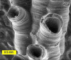 SEM image of a hederelloid from the Devonian of Michigan (largest tube diameter is 0.75 mm). The SEM is used extensively for capturing detailed images of micro and macro fossils.
 Backscattered electron (BSE) image of an antimony-rich region in a fragment of ancient glass. Museums use SEMs for studying valuable artifacts in a nondestructive manner.
 SEM image of the corrosion layer on the surface of an ancient glass fragment; note the laminar structure of the corrosion layer.
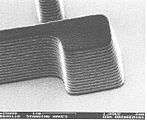 SEM image of a photoresist layer used in semiconductor manufacturing taken on a field emission SEM. These SEMs are important in the semiconductor industry for their high-resolution capabilities.
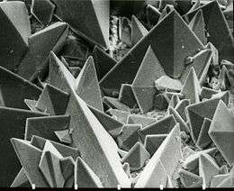
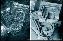
- SEM image of the surface of a kidney stone showing tetragonal crystals of Weddellite (calcium oxalate dihydrate) emerging from the amorphous central part of the stone. Horizontal length of the picture represents 0.5 mm of the figured original.
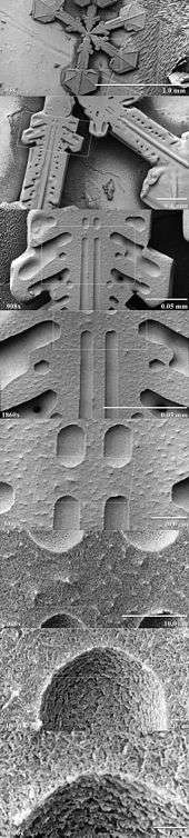
 Two images of the same depth hoar snow crystal, viewed through a light microscope (left) and as an SEM image (right). Note how the SEM image allows for clear perception of the fine structure details which are hard to fully make out in the light microscope image.
 Epidermal cells from the inner surface of an onion flake. Beneath the shagreen-like cell walls one can see nuclei and small organelles floating in the cytoplasm. This BSE-image of a lanthanoid-stained sample was taken without prior fixation, nor dehydration, nor sputtering.
See also
- Applications for electron microscopy
- Electron microscopy
- Energy-dispersive X-ray spectroscopy
- Forensic engineering
- Forensic science
- List of surface analysis methods
- Microscopy
- Teeny Ted from Turnip Town (World's smallest book requires a scanning electron microscope to read).
- Transmission electron microscopy (TEM)
References
- ↑ McMullan, D. (2006). "Scanning electron microscopy 1928–1965". Scanning. 17 (3): 175–185. doi:10.1002/sca.4950170309.
- ↑ McMullan, D. (1988). "Von Ardenne and the scanning electron microscope". Proc Roy Microsc Soc. 23: 283–288.
- ↑ Knoll, Max (1935). "Aufladepotentiel und Sekundäremission elektronenbestrahlter Körper". Zeitschrift für technische Physik. 16: 467–475.
- ↑ von Ardenne M. Improvements in electron microscopes. GB 511204, convention date (Germany) 18 February 1937
- ↑ von Ardenne, Manfred (1938). "Das Elektronen-Rastermikroskop. Theoretische Grundlagen". Zeitschrift für Physik (in German). 109 (9–10): 553–572. Bibcode:1938ZPhy..109..553V. doi:10.1007/BF01341584.
- ↑ von Ardenne, Manfred (1938). "Das Elektronen-Rastermikroskop. Praktische Ausführung". Zeitschrift für technische Physik (in German). 19: 407–416.
- ↑ Zworykin VA, Hillier J, Snyder RL (1942) A scanning electron microscope. ASTM Bull 117, 15–23.
- ↑ McMullan, D. (1953). "An improved scanning electron microscope for opaque specimens". Proceedings of the IEE – Part II: Power Engineering. 100 (75): 245–256. doi:10.1049/pi-2.1953.0095.
- ↑ Oatley CW, Nixon WC, Pease RFW (1965) Scanning electron microscopy. Adv Electronics Electron Phys 21, 181–247.
- ↑ Smith KCA, Oatley, CW (1955). "The scanning electron microscope and its fields of application". British Journal of Applied Physics. 6 (11): 391–399. Bibcode:1955BJAP....6..391S. doi:10.1088/0508-3443/6/11/304.
- ↑ Wells OC (1957) The construction of a scanning electron microscope and its application to the study of fibres. PhD Dissertation, Cambridge University.
- ↑ Suzuki, E. (2002). "High-resolution scanning electron microscopy of immunogold-labelled cells by the use of thin plasma coating of osmium". Journal of Microscopy. 208 (3): 153–157. doi:10.1046/j.1365-2818.2002.01082.x.
- ↑ Seligman, Arnold M.; Wasserkrug, Hannah L.; Hanker, Jacob S. (1966). "A new staining method for enhancing contrast of lipid-containing membranes and droplets in osmium tetroxide-fixed tissue with osmiophilic thiocarbohydrazide (TCH)". Journal of Cell Biology. 30 (2): 424–432. doi:10.1083/jcb.30.2.424. PMC 2106998
 . PMID 4165523.
 - ↑ Malick, Linda E.; Wilson, Richard B.; Stetson, David (1975). "Modified Thiocarbohydrazide Procedure for Scanning Electron Microscopy: Routine use for Normal, Pathological, or Experimental Tissues". Biotechnic & Histochemistry. 50 (4): 265–269. doi:10.3109/10520297509117069.
- ↑ Hortolà, Policarp (2005). "SEM Examination of Human Erythrocytes in Uncoated Bloodstains on Stone: Use of Conventional as Environmental-like SEM in a Soft Biological Tissue (and Hard Inorganic Material)". Journal of Microscopy. 218 (2): 94–103. doi:10.1111/j.1365-2818.2005.01477.x.
- ↑ Hortolà, Policarp (2015). "Evaluating the Use of Synthetic Replicas for SEM Identification of Bloodstains (with Emphasis on Archaeological and Ethnographic Artifacts)". Microscopy and Microanalysis. First View (6): 1504. doi:10.1017/S1431927615014920.
- ↑ Conrad, Cyler; Jones, Emily Lena; Newsome, Seth D.; Schwartz, Douglas W. (2016). "Bone isotopes, eggshell and turkey husbandry at Arroyo Hondo Pueblo". Journal of Archaeological Science: Reports.
- 1 2 3 Jeffree, C. E.; Read, N. D. (1991). "Ambient- and Low-temperature scanning electron microscopy". In Hall, J. L.; Hawes, C. R. Electron Microscopy of Plant Cells. London: Academic Press. pp. 313–413. ISBN 0-12-318880-6.
- ↑ Karnovsky, M. J. (1965). "A formaldehyde-glutaraldehyde fixative of high osmolality for use in electron microscopy" (PDF). Journal of Cell Biology. 27 (2): 137A. JSTOR 1604673.
- ↑ Kiernan, J. A. (2000). "Formaldehyde, formalin, paraformaldehyde and glutaraldehyde: What they are and what they do". Microscopy Today. 2000 (1): 8–12.
- ↑ Russell, S. D.; Daghlian, C. P. (1985). "Scanning electron microscopic observations on deembedded biological tissue sections: Comparison of different fixatives and embedding materials". Journal of Electron Microscopy Technique. 2 (5): 489–495. doi:10.1002/jemt.1060020511.
- ↑ Faulkner, Christine; et al. (2008). "Peeking into Pit Fields: A Multiple Twinning Model of Secondary Plasmodesmata Formation in Tobacco". Plant Cell. 20 (6): 1504–18. doi:10.1105/tpc.107.056903. PMC 2483367. PMID 18667640.
- ↑ Wergin, W. P.; Erbe, E. F. (1994). "Snow crystals: capturing snow flakes for observation with the low-temperature scanning electron microscope". Scanning. 16 (Suppl. IV): IV88.
- ↑ Barnes, P. R. F.; Mulvaney, R.; Wolff, E. W.; Robinson, K. A. (2002). "A technique for the examination of polar ice using the scanning electron microscope". Journal of Microscopy. 205 (2): 118–124. doi:10.1046/j.0022-2720.2001.00981.x. PMID 11879426.
- ↑ Hindmarsh, J. P.; Russell, A. B.; Chen, X. D. (2007). "Fundamentals of the spray freezing of foods—microstructure of frozen droplets". Journal of Food Engineering. 78 (1): 136–150. doi:10.1016/j.jfoodeng.2005.09.011.
- 1 2 Goldstein, G. I.; Newbury, D. E.; Echlin, P.; Joy, D. C.; Fiori, C.; Lifshin, E. (1981). Scanning electron microscopy and x-ray microanalysis. New York: Plenum Press. ISBN 0-306-40768-X.
- ↑ Everhart, T. E.; Thornley, R. F. M. (1960). "Wide-band detector for micro-microampere low-energy electron currents". Journal of Scientific Instruments. 37 (7): 246–248. Bibcode:1960JScI...37..246E. doi:10.1088/0950-7671/37/7/307.
- ↑ Hitachi Launches World’s Highest Resolution FE-SEM. Nanotech Now. 31 May 2011.
- ↑ Danilatos, G. D. (1988). "Foundations of environmental scanning electron microscopy". Advances in Electronics and Electron Physics. Advances in Electronics and Electron Physics. 71: 109–250. doi:10.1016/S0065-2539(08)60902-6. ISBN 9780120146710.
- ↑ US patent 4823006, Danilatos, Gerasimos D. and Lewis, George C., "Integrated electron optical/differential pumping/imaging signal detection system for an environmental scanning electron microscope", issued 1989-4-18
- ↑ Danilatos, G. D. (1990). "Theory of the Gaseous Detector Device in the ESEM". Advances in Electronics and Electron Physics. Advances in Electronics and Electron Physics. 78: 1–102. doi:10.1016/S0065-2539(08)60388-1. ISBN 9780120146789.
- ↑ US patent 4785182, Mancuso, James F.; Maxwell, William B. and Danilatos, Gerasimos D., "Secondary Electron Detector for Use in a Gaseous Atmosphere", issued 1988-11-15
- ↑ History of Electron Microscopy 1990s. sfc.fr
- ↑ Klein, Tobias; Buhr, Egbert; Frase, Carl G. (2012). "TSEM: A Review of Scanning Electron Microscopy in Transmission Mode and Its Applications". Advances in Imaging and Electron Physics. Advances in Imaging and Electron Physics. 171: 297–356. doi:10.1016/B978-0-12-394297-5.00006-4. ISBN 9780123942975.
- ↑ Burgess, Jeremy (1987). Under the Microscope: A Hidden World Revealed. CUP Archive. p. 11. ISBN 0521399408.
- ↑ Showing your true colors, 3D and color in electron microscopy in Lab News magazine
- ↑ Hortolà, P. (2010). "Using digital color to increase the realistic appearance of SEM micrographs of bloodstains". Micron. 41 (7): 904–908. doi:10.1016/j.micron.2010.06.010. PMID 20638857.
- ↑ "Introduction to Electron Microscopy" (PDF). FEI Company. p. 15. Retrieved 12 December 2012.
- ↑ "Next Monday, Digital Surf to Launch Revolutionary SEM Image Colorization". AZO Materials. Retrieved 23 January 2016.
- ↑ Antonovsky, A. (1984). "The application of colour to SEM imaging for increased definition". Micron and Microscopica Acta. 15 (2): 77–84. doi:10.1016/0739-6260(84)90005-4.
- ↑ Danilatos, G.D. (1986). "Colour micrographs for backscattered electron signals in the SEM". Scanning. 9 (3): 8–18. doi:10.1111/j.1365-2818.1986.tb04287.x.
- ↑ Danilatos, G.D. (1986). "Environmental scanning electron microscopy in colour". J. Microscopy. 142: 317–325. doi:10.1002/sca.4950080104.
- ↑ Bertazzo, S.; Gentleman, E.; Cloyd, K. L.; Chester, A. H.; Yacoub, M. H.; Stevens, M. M. (2013). "Nano-analytical electron microscopy reveals fundamental insights into human cardiovascular tissue calcification". Nature Materials. 12 (6): 576–583. doi:10.1038/nmat3627. PMID 23603848.
- ↑ Bertazzo, Sergio; Maidment, Susannah C. R.; Kallepitis, Charalambos; Fearn, Sarah; Stevens, Molly M.; Xie, Hai-nan (9 June 2015). "Fibres and cellular structures preserved in 75-million–year-old dinosaur specimens". Nature Communications. 6: 7352. doi:10.1038/ncomms8352. PMC 4468865. PMID 26056764.
- ↑ Baghaei Rad, Leili (2007). "Computational Scanning Electron Microscopy". International Conference on Frontiers of Characterization and Metrology.
- ↑ Baghaei Rad, Leili; Downes, Ian; Ye, Jun; Adler, David; Pease, R. Fabian W. (2007). "Economic approximate models for backscattered electrons". Journal of Vacuum Science and Technology. 25 (6): 2425. Bibcode:2007JVSTB..25.2425B. doi:10.1116/1.2794068.
- ↑ Hortolà, Policarp (2010). "Generating 3D and 3D-like animations of strongly uneven surface microareas of bloodstains from small series of partially out-of-focus digital SEM micrographs". Micron. 41 (1): 1–6. doi:10.1016/j.micron.2009.04.012. PMID 19631553.
- ↑ Tahmasebi, Pejman; Javadpour, Farzam; Sahimi, Muhammad (2015). "Multiscale and multiresolution modeling of shales and their flow and morphological properties". Scientific Reports. 5: 16373. doi:10.1038/srep16373. PMC 4642334. PMID 26560178.
- ↑ Tahmasebi, Pejman; Javadpour, Farzam; Sahimi, Muhammad (2015). "Three-Dimensional Stochastic Characterization of Shale SEM Images". Transport in Porous Media. 110 (3): 521–531. doi:10.1007/s11242-015-0570-1.
- ↑ Tahmasebi, Pejman; Sahimi, Muhammad (2012). "Reconstruction of three-dimensional porous media using a single thin section". Physical Review E. 85 (6). doi:10.1103/PhysRevE.85.066709.
External links
| Library resources about Scanning electron microscopy |
| Wikibooks has a book on the topic of: Nanotechnology |
| Wikimedia Commons has media related to Scanning electron microscope. |
| Wikimedia Commons has media related to Scanning electron microscopic images. |
- General
- HowStuffWorks – How Scanning Electron Microscopes Work
- Notes on the SEM Notes covering all aspects of the SEM
- Scanning Electron Microscopy basics an animated tutorial on how SEM works
- Virtual SEM – sparkler. Interactive simulation of a scanning electron microscope (SEM)
- Preparing a Sample for the SEM preparing a non-conducting subject for the SEM (QuickTime-movie)
- multichannel color SEM imaging and
- DDC-SEM image examples
- Video on the scanning electron microscope, Karlsruhe University of Applied Sciences
- animations and explanations on various types of microscopes including electron microscopes (Université Paris Sud)
- History
- Microscopy History links from the University of Alabama Department of Biological Sciences
- Environmental Scanning Electron Microscope (ESEM) history
- Images
- Rippel Electron Microscope Facility Many dozens of (mostly biological) SEM images from Dartmouth College.
- Lanthanoid staining SEM images from Research Institute of Eye Diseases, Moscow.