Power semiconductor device
A power semiconductor device is a semiconductor device used as a switch or rectifier in power electronics; a switch-mode power supply is an example. Such a device is also called a power device or, when used in an integrated circuit, a power IC.
A power semiconductor device is usually used in "commutation mode" (i.e., it is either on or off), and therefore has a design optimized for such usage; it should usually not be used in linear operation.
History
The first power semiconductor device appeared in 1952 with the introduction of the power diode by R.N. Hall. It was made of germanium and had a reverse voltage blocking capability of 200 V and a current rating of 35 A.
The thyristor appeared in 1957. It is able to withstand very high reverse breakdown voltage and is also capable of carrying high current. However, one disadvantage of the thyristor in switching circuits is that once it becomes 'latched-on' in the conducting state; it cannot be turned off by external control, as the thyristor turn-off is passive, i.e., the power must be disconnected from the device. Thyristors which could be turned off, called gate turn-off thyristors (GTO), were introduced in 1960.[1] These overcome some limitations of the ordinary thyristor, because they can be turned on or off with an applied signal.
The first bipolar transistor device with substantial power handling capabilities was introduced in the 1948 by William Shockley.
Due to improvements in the MOSFET technology (metal oxide semiconductor technology, initially developed to produce integrated circuits), the power MOSFET became available in the late 1970s. International Rectifier introduced a 25 A, 400 V power MOSFET in 1978.[2] This device allows operation at higher frequencies than a bipolar transistor, but is limited to low voltage applications.
The Insulated-gate bipolar transistor (IGBT) was developed in the 1980s, and became widely available in the 1990s. This component has the power handling capability of the bipolar transistor and the advantages of the isolated gate drive of the power MOSFET.
Common devices
Some common power devices are the power diode, thyristor, power MOSFET, and IGBT. The power diode and power MOSFET operate on similar principles to their low-power counterparts, but are able to carry a larger amount of current and are typically able to support a larger reverse-bias voltage in the off-state.
Structural changes are often made in a power device in order to accommodate the higher current density, higher power dissipation, and/or higher reverse breakdown voltage. The vast majority of the discrete (i.e., non-integrated) power devices are built using a vertical structure, whereas small-signal devices employ a lateral structure. With the vertical structure, the current rating of the device is proportional to its area, and the voltage blocking capability is achieved in the height of the die. With this structure, one of the connections of the device is located on the bottom of the semiconductor die.
Classifications
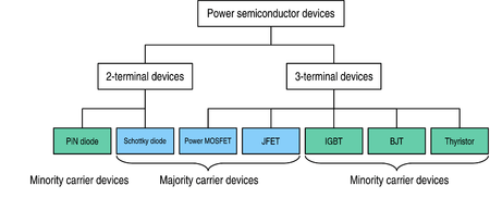
A power device may be classified as one of the following main categories (see figure 1):
- A two-terminal device (e.g., a diode), whose state is completely dependent on the external power circuit to which it is connected.
- A three-terminal device (e.g., a triode), whose state is dependent on not only its external power circuit, but also the signal on its driving terminal (this terminal is known as the gate or base).
Another classification is less obvious, but has a strong influence on device performance:
- A majority carrier device (e.g., a Schottky diode, a MOSFET, etc.); this uses only one type of charge carriers.
- A minority carrier device (e.g., a thyristor, a bipolar transistor, an IGBT, etc.); this uses both majority and minority carriers (i.e., electrons and electron holes).
A majority carrier device is faster, but the charge injection of minority carrier devices allows for better on-state performance.
Diodes
An ideal diode should have the following characteristics:
- When forward-biased, the voltage across the end terminals of the diode should be zero, whatever the current that flows through it (on-state).
- When reverse-biased, the leakage current should be zero, whatever the voltage (off-state).
- The transition (or commutation) between the on-state and the off-state should be instantaneous.
In reality, the design of a diode is a trade-off between performance in on-state, off-state, and commutation. Indeed, the same area of the device must sustain the blocking voltage in the off-state and allow current flow in the on-state; as the requirements for the two states are completely opposite, a diode has to be either optimised for one of them, or time must be allowed to switch from one state to the other (i.e., the commutation speed must be reduced).
These trade-offs are the same for all power devices; for instance, a Schottky diode has excellent switching speed and on-state performance, but a high level of leakage current in the off-state. On the other hand, a PIN diode is commercially available in different commutation speeds (what are called "fast" and "ultrafast" rectifiers), but any increase in speed is necessarily associated with a lower performance in the on-state.
Switches

The trade-offs between voltage, current, and frequency ratings also exist for a switch. In fact, any power semiconductor relies on a PIN diode structure in order to sustain voltage; this can be seen in figure 2. The power MOSFET has the advantages of a majority carrier device, so it can achieve a very high operating frequency, but it cannot be used with high voltages; as it is a physical limit, no improvement is expected in the design of a silicon MOSFET concerning its maximum voltage ratings. However, its excellent performance in low voltage applications make it the device of choice (actually the only choice, currently) for applications with voltages below 200 V. By placing several devices in parallel, it is possible to increase the current rating of a switch. The MOSFET is particularly suited to this configuration, because its positive thermal coefficient of resistance tends to result in a balance of current between the individual devices.
The IGBT is a recent component, so its performance improves regularly as technology evolves. It has already completely replaced the bipolar transistor in power applications; a power module is available in which several IGBT devices are connected in parallel, making it attractive for power levels up to several megawatts, which pushes further the limit at which thyristors and GTOs become the only option. Basically, an IGBT is a bipolar transistor driven by a power MOSFET; it has the advantages of being a minority carrier device (good performance in the on-state, even for high voltage devices), with the high input impedance of a MOSFET (it can be driven on or off with a very low amount of power).
The major limitation of the IGBT for low voltage applications is the high voltage drop it exhibits in the on-state (2-to-4 V). Compared to the MOSFET, the operating frequency of the IGBT is relatively low (usually not higher than 50 kHz), mainly because of a problem during turn-off known as current-tail: The slow decay of the conduction current during turn-off results from a slow recombination of a large number of carriers that flood the thick 'drift' region of the IGBT during conduction. The net result is that the turn-off switching loss of an IGBT is considerably higher than its turn-on loss. Generally, in datasheets, turn-off energy is mentioned as a measured parameter; that number has to be multiplied with the switching frequency of the intended application in order to estimate the turn-off loss.
At very high power levels, a thyristor-based device (e.g., a SCR, a GTO, a MCT, etc.) is still the only choice. This device can be turned on by a pulse provided by a driving circuit, but cannot be turned off by removing the pulse. A thyristor turns off as soon as no more current flows through it; this happens automatically in an alternating current system on each cycle, or requires a circuit with the means to divert current around the device. Both MCTs and GTOs have been developed to overcome this limitation, and are widely used in power distribution applications.
Parameters


- Breakdown voltage: Often, there is a trade-off between breakdown voltage rating and on-resistance, because increasing the breakdown voltage by incorporating a thicker and lower doped drift region leads to a higher on-resistance.
- On-resistance: A higher current rating lowers the on-resistance due to greater numbers of parallel cells. This increases overall capacitance and slows down the speed.
- Rise and fall times: The amount of time it takes to switch between the on-state and the off-state.
- Safe-operating area: This is a thermal dissipation and "latch-up" consideration.
- Thermal resistance: This is an often ignored but extremely important parameter from the point of view of practical design; a semiconductor does not perform well at elevated temperature, and yet due to large current conduction, a power semiconductor device invariably heats up. Therefore, such a devices needs to be cooled by removing that heat continuously; packaging and heatsink technology provide a means for removing heat from a semiconductor device by conducting it to the external environment. Generally, a large current device has a large die and packaging surface areas and lower thermal resistance.
Research and development
Packaging
The role of packaging is to:
- connect a die to the external circuit.
- provide a way to remove the heat generated by the device.
- protect the die from the external environment (moisture, dust, etc.).
Many of the reliability issues of a power device are either related to excessive temperature or fatigue due to thermal cycling. Research is currently carried out on the following topics:
- Cooling performance.
- Resistance to thermal cycling by closely matching the Coefficient of thermal expansion of the packaging to that of the silicon.
- The maximum operating temperature of the packaging material.
Research is also ongoing on electrical issues such as reducing the parasitic inductance of packaging; this inductance limits the operating frequency, because it generates losses during commutation.
A low-voltage MOSFET is also limited by the parasitic resistance of its package, as its intrinsic on-state resistance can be as low as one or two milliohms.
Some of the most common type of power semiconductor packages include the TO-220, TO-247, TO-262, TO-3, D2Pak, etc.
Improvement of structures
The IGBT design is still under development and can be expected to provide increases in operating voltages. At the high-power end of the range, the MOS-controlled thyristor is a promising device. Achieving a major improvement over the conventional MOSFET structure by employing the super junction charge-balance principle: essentially, it allows the thick drift region of a power MOSFET to be heavily doped, thereby reducing the electrical resistance to electron flow without compromising the breakdown voltage. This is juxtaposed with a region that is similarly doped with the opposite carrier polarity (holes); these two similar, but oppositely doped regions effectively cancel out their mobile charge and develop a 'depleted region' that supports the high voltage during the off-state. On the other hand, during the on-state, the higher doping of the drift region allows for the easy flow of carriers, thereby reducing on-resistance. Commercial devices, based on this super junction principle, have been developed by companies like Infineon (CoolMOSTM products) and International Rectifier (IR).
Wide band-gap semiconductors
The major breakthrough in power semiconductor devices is expected from the replacement of silicon by a wide band-gap semiconductor. At the moment, silicon carbide (SiC) is considered to be the most promising. A SiC Schottky diode with a breakdown voltage of 1200 V is commercially available, as is a 1200 V JFET. As both are majority carrier devices, they can operate at high speed. A bipolar device is being developed for higher voltages (up to 20 kV). Among its advantages, silicon carbide can operate at a higher temperature (up to 400 °C) and has a lower thermal resistance than silicon, allowing for better cooling.
See also
- Bipolar junction transistor
- Bootstrapping
- FGMOS
- Dimmer
- Gate turn-off thyristor
- Integrated gate-commutated thyristor
- TRIAC
- Voltage regulator
- MOSFET
- SCR
Notes and references
Notes
References
- Baliga, B. Jayant. Power Semiconductor Devices. Boston: PWS publishing Company. ISBN 0-534-94098-6.
- Jain, Alok. Power Electronics and Its Applications. Mumbai: Penram International Publishing. ISBN 81-87972-22-X.
- Semikron: Application Manual IGBT and MOSFET Power Modules, 2. Edition, 2015,ISLE Verlag, ISBN 978-3-938843-83-3 PDF-Version
- Arendt Wintrich; Ulrich Nicolai; Werner Tursky; Tobias Reimann (2010) (in German), Applikationshandbuch 2015 (2. ed.), ISLE Verlag, ISBN 978-3-938843-83-3, https://www.semikron.com/dl/service-support/downloads/download/semikron-applikationshandbuch-leistungshalbleiter-de-2015-08-04.pdf
- Arendt Wintrich; Ulrich Nicolai; Werner Tursky; Tobias Reimann (2015). Application Manual 2015 (PDF-Version) (2. ed.). ISLE Verlag. ISBN 978-3-938843-83-3.
External links
- A review on Power Semiconductor Devices
- Interactive Power Electronics Seminar (iPES)
- Powerguru.org – power electronics knowledge base with training material