Platform Controller Hub

The Platform Controller Hub (PCH) is a family of Intel microchips, introduced circa 2008. It is the successor to the previous Intel Hub Architecture, which used a northbridge and southbridge instead, and first appeared in the Intel 5 Series.
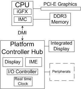
The PCH controls certain data paths and support functions used in conjunction with Intel CPUs. These include clocking (the system clock), Flexible Display Interface (FDI) and Direct Media Interface (DMI), although FDI is only used when the chipset is required to support a processor with integrated graphics. As such, I/O functions are reassigned between this new central hub and the CPU compared to the previous architecture: some northbridge functions, the memory controller and PCI-e lanes, were integrated into the CPU while the PCH took over the remaining functions in addition to the traditional roles of the southbridge.
Overview
The PCH architecture supersedes Intel's previous Hub Architecture, with its design addressing the eventual problematic performance bottleneck between the processor and the motherboard. Over time, the speed of CPUs kept increasing but the bandwidth of the front-side bus (FSB) (connection between the CPU and the motherboard) did not, resulting in a performance bottleneck.[1]
Under the Hub Architecture, a motherboard would have a two piece chipset consisting of a northbridge chip and a southbridge chip. As a solution to the bottleneck, several functions belonging to the traditional northbridge and southbridge chipsets were rearranged. The northbridge is now eliminated completely and its functions, the memory controller and PCI Express lanes for expansion cards, are now incorporated into the CPU die or package.
The PCH then incorporates a few of the remaining northbridge functions (e.g. clocking) in addition to all of the southbridge's functions. The system clock was previously a connection and is now fused in with the PCH. Two different connections exist between the PCH and the CPU: Flexible Display Interface (FDI) and Direct Media Interface (DMI). The FDI is only used when the chipset requires supporting a processor with integrated graphics. The Intel Management Engine was also moved to the PCH starting with the Nehalem processors and 5-Series chipsets.
With the northbridge functions integrated to the CPU, much of the bandwidth needed for chipsets is now relieved.
This style began in Nehalem and will remain for the foreseeable future, through Cannonlake.
Phase-out
Beginning with ultra-low-power Broadwells and continuing with mobile Skylake processors, Intel incorporated the clock, PCI controller, and southbridge IO controllers into the CPU package, eliminating the PCH for a system on a chip (SOC) design. Rather than DMI, these SOCs directly expose PCIe lanes, as well as SATA, USB, and HDA lines from integrated controllers, and SPI/I²C/UART/GPIO lines for sensors. Like PCH-compatible CPUs, they continue to expose DisplayPort, RAM, and SMBus lines. However, a fully integrated voltage regulator will be absent until Cannonlake.
Ibex Peak
The Intel 5 Series chipsets were the first to introduce a PCH. This first PCH is codenamed Ibex Peak.
This has the following variations:
- BD3400 (PCH 3400) Server
- BD3420 (PCH 3420) Server
- BD3450 (PCH 3450) Server
- BD82P55 (PCH P55) Desktop Base
- BD82H55 (PCH H55) Desktop Home
- BD82H57 (PCH H57) Desktop Home
- BD82Q57 (PCH Q57) Desktop Office
- BD82PM55 (PCH PM55) Mobile Base
- BD82HM55 (PCH HM55) Mobile Home
- BD82HM57 (PCH HM57) Mobile Home
- BD82QM57 (PCH QM57) Mobile Office
- BD82QS57 (PCH QS57) Mobile SFF
Issues
- Bogus USB ports will be detected by desktop PCHs equipped with 6 USB ports (3420, H55) on the first EHCI controller. This can happen when AC power is removed after entering ACPI S4. Applying AC power back and resuming from S4 may result in non detected or even non functioning USB device (erratum 12)
- Bogus USB ports will be detected by mobile PCH equipped with 6 USB ports (HM55) on the first EHCI controller. This can happen when AC power and battery are removed after entering ACPI S4. Applying AC power or battery back and resuming from S4 may result in non detected or even non functioning USB device (erratum 13)
- Reading the HPET comparator timer immediately after a write returns the old value (erratum 14)
- SATA 6Gbit/s devices may not be detected at cold boot or after ACPI S3, S4 resume (erratum 21)
Langwell
Langwell is the codename of a PCH in the Moorestown MID/smartphone platform.[2][3] for Atom Lincroft microprocessors.
This has the following variations:
- AF82MP20 (PCH MP20)
- AF82MP30 (PCH MP30)
Tiger Point
Tiger Point is the codename of a PCH in the Pine Trail netbook platform chipset for Atom Pineview microprocessors.
This has the following variations:
- CG82NM10 (PCH NM10)
Topcliff
Topcliff is the codename of a PCH in the Queens Bay embedded platform chipset for Atom Tunnel Creek microprocessors.
It connects to the processor via PCI-E (vs. DMI as other PCHs do).
This has the following variations:
- CS82TPCF (PCH EG20T)
Cougar Point
Cougar Point is the codename of a PCH in Intel 6 Series chipsets for mobile, desktop, and workstation / server platforms. It is most closely associated with Sandy Bridge processors.
This has the following variations:
- BD82C202 (PCH C202) Server
- BD82C204 (PCH C204) Server
- BD82C206 (PCH C206) Workstation / Server
- BD82P67 (PCH P67) Desktop Base
- BD82H67 (PCH H67) Desktop Home
- BD82H61 (PCH H61) Desktop Home
- BD82Z68 (PCH Z68) Combined desktop base and home
- BD82B65 (PCH B65) Desktop Office
- BD82Q67 (PCH Q67) Desktop Office
- BD82HM65 (PCH HM65) Mobile Home
- BD82HM67 (PCH HM67) Mobile Home
- BD82QM67 (PCH QM67) Mobile Office
- BD82QS67 (PCH QS67) Mobile SFF
- BD82UM67 (PCH UM67) Ultra Mobile
Issues
In the first month after Cougar Point's release, January 2011, Intel posted a press release stating a design error had been discovered. Specifically, a transistor in the 3 Gbit/s PLL clocking tree was receiving too high voltage. The projected result was a 5–15% failure rate within three years of 3 Gbit/s SATA ports, commonly used for storage devices such as hard drives and optical drives. Through OEMs, Intel plans to repair or replace all affected products at a cost of $700 million.[4][5]
Whitney Point
Whitney Point is the codename of a PCH in the Oak Trail tablet platform for Atom Lincroft microprocessors.
This has the following variations:
- 82SM35 (PCH SM35)
Panther Point
Panther Point is the codename of a PCH in Intel 7 Series chipsets for mobile and desktop. It is most closely associated with Ivy Bridge processors. These chipsets have integrated USB 3.0.[6]
This has the following variations:
- BD82C216 (PCH C216) Workstation/Server
- BD82H77 (PCH H77) Desktop Home
- BD82Z77 (PCH Z77) Combined desktop base and home
- BD82Z75 (PCH Z75) Combined desktop base and home
- BD82B75 (PCH B75) Desktop Office
- BD82Q77 (PCH Q77) Desktop Office
- BD82Q75 (PCH Q75) Desktop Office
- BD82HM77 (PCH HM77) Mobile Home
- BD82HM76 (PCH HM76) Mobile Home
- BD82HM75 (PCH HM75) Mobile Home
- BD82HM70 (PCH HM70) Mobile Home
- BD82QM77 (PCH QM77) Mobile Office
- BD82QS77 (PCH QS77) Mobile Office
- BD82UM77 (PCH UM77) Ultra Mobile
Cave Creek
Cave Creek is the codename of the PCH most closely associated with Crystal Forest platforms and Gladden[7] or Sandy Bridge-EP/EN[8] processors.
- DH8900 (PCH 8900) Communications
- DH8903 (PCH 8903) Communications
- DH8910 (PCH 8910) Communications
- DH8920 (PCH 8920) Communications
Patsburg
Patsburg is the codename of a PCH in Intel 7 Series chipsets for server and workstation using the LGA 2011 socket. It was initially launched in 2011 as part of Intel X79 for the desktop enthusiast Sandy Bridge-E processors in Waimea Bay platforms.[9] Patsburg was then used for the Sandy Bridge-EP server platform (the platform was codenamed Romley and the CPUs codenamed Jaketown, and finally branded as Xeon E5-2600 series) launched in early 2012.[10]
Launched in the fall of 2013, the Ivy Bridge-E/EP processors (the latter branded as Xeon E5-2600 v2 series) also work with Patsburg, typically with a BIOS update.[11][12]
Patsburg has the following variations:
- BD82C602 (PCH C602) Server
- BD82C602J (PCH C602J) Server
- BD82C604 (PCH C604) Server
- BD82C606 (PCH C606) Workstation / Server
- BD82C608 (PCH C608) Workstation / Server
- BD82X79 (PCH X79) Workstation
Coleto Creek
Coleto Creek is the codename of the PCH most closely associated with Highland Forest platforms and Ivy Bridge-EP[13] processors.
- DH8925 (PCH 8925) Communications
- DH8926 (PCH 8926) Communications
- DH8950 (PCH 8950) Communications
- DH8955 (PCH 8955) Communications
Lynx Point
Lynx Point is the codename of a PCH in Intel 8 Series chipsets, most closely associated with Haswell processors with LGA 1150 socket.[14] The Lynx Point chipset connects to the processor primarily over the Direct Media Interface (DMI) interface.[15]
The following variants are available:[16]
- DH82C222 (PCH C222) Workstation/Server
- DH82C224 (PCH C224) Workstation/Server
- DH82C226 (PCH C226) Workstation/Server
- DH82H81 (PCH H81) Desktop Home
- DH82H87 (PCH H87) Desktop Home
- DH82Z87 (PCH Z87) Combined desktop base and home
- DH82B85 (PCH B85) Desktop Office
- DH82Q87 (PCH Q87) Desktop Office
- DH82Q85 (PCH Q85) Desktop Office
- DH82HM87 (PCH HM87) Mobile Home
- DH82HM86 (PCH HM86) Mobile Home
- DH82QM87 (PCH QM87) Mobile Office
In addition the following newer variants are available, additionally known as Wildcat Point, which also support Haswell Refresh processors:[17]
Issues
A design flaw causes devices connected to the Lynx Point's integrated USB 3.0 controller to be disconnected when the system wakes up from the S3 state (Suspend to RAM), forcing the USB devices to be reconnected although no data is lost.[18][19] This issue is corrected in C2 stepping level of the Lynx Point chipset.[20]
Wellsburg
Wellsburg is the codename for the C610-series PCH, supporting the Haswell-E (Core i7 Extreme), Haswell-EP (Xeon E5-16xx v3 and Xeon E5-26xx v3), and Broadwell-EP (Xeon E5-26xx v4) processors. Generally similar to Patsburg, Wellsburg consumes only up to 7 W when fully loaded.[21]
Wellsburg has the following variations:
- DH82029 (PCH C612), intended for servers and workstations
- DHX99 (PCH X99), intended for workstations
Sunrise Point
Sunrise Point is the codename of a PCH in Intel 100 Series chipsets, most closely associated with Skylake processors with LGA 1151 socket.
The following variants are available:[22]
- GL82C236 (PCH C236) Workstation/Server
- GL82H110 (PCH H110) Desktop Home
- GL82H170 (PCH H170) Desktop Home
- GL82Z170 (PCH Z170) Combined desktop base and home
- GL82B150 (PCH B150) Desktop Office
- GL82Q150 (PCH Q150) Desktop Office
- GL82Q170 (PCH Q170) Desktop Office
- GL82HM170 (PCH HM170) Mobile Home
- GL82CM236 (PCH CM236) Mobile Workstation
- GL82QM170 (PCH QM170) Mobile Office
See also
- List of Intel chipsets
- System Controller Hub (SCH)
- I/O Controller Hub (ICH)
- PCI IDE ISA Xcelerator (PIIX)
References
- ↑ Hook, Brian. "Breaking the Speed Barrier: The Frontside Bus Bottleneck". Technewsworld. Retrieved 1 February 2016.
- ↑ Langwell Background Information, Intel, retrieved 2010-08-03
- ↑ New Intel Atom Processor-Based Platform Using Significantly Lower Power Readies Intel for Smartphone, Tablet Push, Intel, May 4, 2010, retrieved 2010-07-27
- ↑ Intel Identifies Chipset Design Error, Implementing Solution, Intel, 31 January 2011
- ↑ The Source of Intel's Cougar Point SATA Bug, AnandTech, 31 January 2011
- ↑ "Correction: Ivy Bridge and Thunderbolt - Featured, not Integrated". AnandTech. Retrieved 2014-01-21.
- ↑ (2:48) (2014-01-13). "Intel Xeon/Core/Pentium/Celeron, Communications Chipset 89xx". Intel. Retrieved 2014-01-21.
- ↑ "Intel Xeon Processor E5-2600/E5-2400/Communications Chipset 89xx". Ssl.intel.com. Retrieved 2014-01-21.
- ↑ "A Look Into Intel's Next Gen Enthusiast Platform : Sandy Bridge E & Waimea Bay", vr-zone.com, April 15, 2010, archived from the original on April 23, 2010, retrieved 2010-07-27
- ↑ "Intel plugs both your sockets with 'Jaketown' Xeon E5-2600s • The Channel". Channelregister.co.uk. 2012-03-06. Retrieved 2014-01-21.
- ↑ "Ivy Bridge-E Not a Cut-down 8-core, 20 MB LLC Die". techPowerUp.com. 2013-08-12. Retrieved 2014-01-21.
- ↑ http://www.theregister.co.uk/2013/09/10/intel_ivy_bridge_xeon_e5_2600_v2_launch/
- ↑ "Intel Announces Highland Forest, a New Platform that will Accelerate Network Transformation". Intel. 2013-12-04. Retrieved 2014-08-09.
- ↑ Shawn Knight (2012-11-13). "Leaked Intel slides detail Haswell's Lynx Point chipset". techspot.com. Retrieved 2013-10-30.
- ↑ "Intel "Lynx Point" 8-series Chipset Detailed, Completely SATA 6 Gbit/s". techpowerup.com. 2012-02-17. Retrieved 2013-10-30.
- ↑ "Products (Formerly Lynx Point)". Intel. Retrieved 2013-10-30.
- ↑ Andrew Cunningham (2014-05-11). "New Intel chipsets speed up your storage, but they're missing new CPUs". arstechnica.com. Retrieved 2014-05-13.
- ↑ "Lynx Point USB 3.0 Controller Issue Correction Needs New Hardware". techpowerup.com. 2013-03-11. Retrieved 2013-10-30.
- ↑ Frank Everaardt (2013-03-01). "USB 3.0 problems for Intel's Haswell". hardware.info. Retrieved 2013-10-30.
- ↑ "Haswell C2 stepping availability". arstechnica.com. 2013. Retrieved 2013-10-30.
- ↑ "Intel Readies 18-Core Xeon "Broadwell-EP" Microprocessors for Launch in 2015 – Report". xbitlabs.com. Retrieved 2014-01-21.
- ↑ "Products (Formerly Skylake)". Intel. Retrieved 2015-10-24.