Plasmonic solar cell
A Plasmonic solar cell is a type of thin film solar cell that converts light into electricity with the assistance of plasmons.[1] They are typically less than 2 μm thick and theoretically could be as thin as 100 nm.[2] They can use substrates which are cheaper than silicon, such as glass, plastic or steel. One of the challenges for thin film solar cells is that they do not absorb as much light as thicker solar cells made with materials with the same absorption coefficient. Methods for light trapping are important for thin film solar cells.[3] Plasmonic cells improve absorption by scattering light using metal nano-particles excited at their surface plasmon resonance.[4] Incoming light at the plasmon resonance frequency induces electron oscillations at the surface of the nanoparticles. The oscillation electrons can then be captured by a conductive layer producing an electrical current. The voltage produced is dependent on the bandgap of the conductive layer and the potential of the electrolyte in contact with the nanoparticles. There is still considerable research necessary to enable the technology to reach its full potential and commercialization of plasmonic enhanced solar cells.[2]
History
Devices
There are currently three different generations of SCs. The first generation (those in the market today) are made with crystalline semiconductor wafers, typically silicon. These are the SCs everybody thinks of when they hear "Solar Cell".
Current SCs trap light by creating pyramids on the surface which have dimensions bigger than most thin film SCs. Making the surface of the substrate rough (typically by growing SnO2 or ZnO on surface) with dimensions on the order of the incoming wavelengths and depositing the SC on top has been explored. This method increases the photocurrent, but the thin film SC would then have poor material quality. [5]
The second generation SCs are based on thin film technologies such as those presented here. These SCs focus on lowering the amount of material used as well as increasing the energy production. Third generation SCs are currently being researched. They focus on reducing the cost of the second generation SCs. [6] The third generation SCs are discussed in more detail under recent advancement.
Design
The design for a PSC varies depending on the method being used to trap and scatter light across the surface and through the material.
Nanoparticle cells
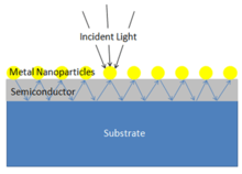
A common design is to deposit metal nano-particles on the top surface of the thin film SC. When light hits these metal nano-particles at their surface plasmon resonance, the light is scattered in many different directions. This allows light to travel along the SC and bounce between the substrate and the nano-particles enabling the SC to absorb more light. [7]
Metal film cells
Other methods utilizing surface plasmons for harvesting solar energy are available. One other type of structure is to have a thin film of silicon and a thin layer of metal deposited on the lower surface. The light will travel through the silicon and generate surface plasmons on the interface of the silicon and metal. This generates electric fields inside of the silicon since electric fields do not travel very far into metals. If the electric field is strong enough, electrons can be moved and collected to produce a photocurrent. The thin film of metal in this design must have nanometer sized grooves which act as waveguides for the incoming light in order to excite as many photons in the silicon thin film as possible. [8]
Principles
General
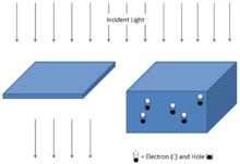
When a photon is excited in the substrate of a SC, an electron and hole are separated. Once the electrons and holes are separated, they will want to recombine since they are of opposite charge. If the electrons can be collected prior to this happening they can be used as a current for an external circuit. Designing the thickness of a solar cell is always a trade-off between minimizing this recombination (thinner layers) and absorbing more photons (thicker layer).[7]
Nano-particles
Scattering and Absorption
The basic principles for the functioning of plasmonic solar cells include scattering and absorption of light due to the deposition of metal nano-particles. Silicon does not absorb light very well. For this reason, more light needs to be scattered across the surface in order to increase the absorption. It has been found that metal nano-particles help to scatter the incoming light across the surface of the silicon substrate. The equations that govern the scattering and absorption of light can be shown as:

This shows the scattering of light for particles which have diameters below the wavelength of light.
![{\displaystyle C_{abs}={\frac {2\pi }{\lambda }}{\text{Im}}[\alpha ]}](../I/m/a69d9da0969957f585f701b8550388a103702ea2.svg)
This shows the absorption for a point dipole model.
![\alpha =3V\left[{\frac {\epsilon _{p}/\epsilon _{m}-1}{\epsilon _{p}/\epsilon _{m}+2}}\right]](../I/m/70ef6bf06476d79a26e139882a3f733eabdfdff4.svg)
This is the polarizability of the particle. V is the particle volume. is the dielectric function of the particle. is the dielectric function of the embedding medium. When the polarizability of the particle becomes large. This polarizability value is known as the surface plasmon resonance. The dielectric function for metals with low absorption can be defined as:


In the previous equation, is the bulk plasma frequency. This is defined as:


N is the density of free electrons, e is the electronic charge and m is the effective mass of an electron. is the dielectric constant of free space. The equation for the surface plasmon resonance in free space can therefore be represented by:


Many of the plasmonic solar cells use nano-particles to enhance the scattering of light. These nano-particles take the shape of spheres, and therefore the surface plasmon resonance frequency for spheres is desirable. By solving the previous equations, the surface plasmon resonance frequency for a sphere in free space can be shown as:

As an example, at the surface plasmon resonance for a silver nanoparticle, the scattering cross-section is about 10x the cross-section of the nanoparticle. The goal of the nano-particles is to trap light on the surface of the SC. The absorption of light is not important for the nanoparticle, rather, it is important for the SC. One would think that if the nanoparticle is increased in size, then the scattering cross-section becomes larger. This is true, however, when compared with the size of the nanoparticle, the ratio () is reduced. Particles with a large scattering cross section tend to have a broader plasmon resonance range.

Wavelength dependence
Surface plasmon resonance mainly depends on the density of free electrons in the particle. The order of densities of electrons for different metals is shown below along with the type of light which corresponds to the resonance.
If the dielectric constant for the embedding medium is varied, the resonant frequency can be shifted. Higher indexes of refraction will lead to a longer wavelength frequency.
Light trapping
The metal nano-particles are deposited at a distance from the substrate in order to trap the light between the substrate and the particles. The particles are embedded in a material on top of the substrate. The material is typically a dielectric, such as silicon or silicon nitride. When performing experiment and simulations on the amount of light scattered into the substrate due to the distance between the particle and substrate, air is used as the embedding material as a reference. It has been found that the amount of light radiated into the substrate decreases with distance from the substrate. This means that nano-particles on the surface are desirable for radiating light into the substrate, but if there is no distance between the particle and substrate, then the light is not trapped and more light escapes.
The surface plasmons are the excitations of the conduction electrons at the interface of metal and the dielectric. Metallic nano-particles can be used to couple and trap freely propagating plane waves into the semiconductor thin film layer. Light can be folded into the absorbing layer to increase the absorption. The localized surface plasmons in metal nano-particles and the surface plasmon polaritons at the interface of metal and semiconductor are of interest in the current research. In recent reported papers, the shape and size of the metal nano-particles are key factors to determine the incoupling efficiency. The smaller particles have larger incoupling efficiency due to the enhanced near-field coupling. However, very small particles suffer from large ohmic losses. [9]
Metal film
As light is incident upon the surface of the metal film, it excites surface plasmons. The surface plasmon frequency is specific for the material, but through the use of gratings on the surface of the film, different frequencies can be obtained. The surface plasmons are also preserved through the use of waveguides as they make the surface plasmons easier to travel on the surface and the losses due to resistance and radiation are minimized. The electric field generated by the surface plasmons influences the electrons to travel toward the collecting substrate. [10]
Materials
| First Generation | Second Generation | Third Generation |
|---|---|---|
| Single-crystal silicon | CuInSe2 | Gallium Indium Phosphide |
| Multicrystalline silicon | amorphous silicon | Gallium Indium Arsenide |
| Polycrystalline silicon | thin film crystalline Si | Germanium |
Applications
The applications for plasmonic solar cells are endless. The need for cheaper and more efficient solar cells is huge. In order for solar cells to be considered cost effective, they need to provide energy for a smaller price than that of traditional power sources such as coal and gasoline. The movement toward a more green world has helped to spark research in the area of plasmonic solar cells. Currently, solar cells cannot exceed efficiencies of about 30% (First Generation). With new technologies (Third Generation), efficiencies of up to 40-60% can be expected. With a reduction of materials through the use of thin film technology (Second Generation), prices can be driven lower.
Certain applications for plasmonic solar cells would be for space exploration vehicles. A main contribution for this would be the reduced weight of the solar cells. An external fuel source would also not be needed if enough power could be generated from the solar cells. This would drastically help to reduce the weight as well.
Solar cells have a great potential to help rural electrification. An estimated two million villages near the equator have limited access to electricity and fossil fuels and that approximately 25%[12] of people in the world do not have access to electricity. When the cost of extending power grids, running rural electricity and using diesel generators is compared with the cost of solar cells, many times the solar cells win. If the efficiency and cost of the current solar cell technology is decreased even further, then many rural communities and villages around the world could obtain electricity when current methods are out of the question. Specific applications for rural communities would be water pumping systems, residential electric supply and street lights. A particularly interesting application would be for health systems in countries where motorized vehicles are not overly abundant. Solar cells could be used to provide the power to refrigerate medications in coolers during transport.
Solar cells could also provide power to lighthouses, buoys, or even battleships out in the ocean. Industrial companies could use them to power telecommunications systems or monitoring and control systems along pipelines or other system.[13]
If the solar cells could be produced on a large scale and be cost effective then entire power stations could be built in order to provide power to the electrical grids. With a reduction in size, they could be implemented on both commercial and residential buildings with a much smaller footprint. They might not even seem like an eyesore. [13]
Other areas are in hybrid systems. The solar cells could help to power high consumption devices such as automobiles in order to reduce the amount of fossil fuels used and to help improve the environmental conditions of the earth.
In consumer electronics devices, solar cells could be used to replace batteries for low power electronics. This would save everyone a lot of money and it would also help to reduce the amount of waste going into landfills.[14]
Recent advancements
Choice of plasmonic metal nano-particles
Proper choice of plasmatic metal nano-particles is crucial for the maximum light absorption in the active layer. Front surface located nano-particles Ag and Au are the most widely used materials due to their surface plasmon resonances located in the visible range and therefore interact more strongly with the peak solar intensity. However, such noble metal nano-particles always introduce reduced light coupling into Si at the short wavelengths below the surface plasmon resonance due to the detrimental Fano effect, i.e. the destructive interference between the scattered and unscattered light. Moreover, the noble metal nano-particles are impractical to implement for large-scale solar cell manufacture due to their high cost and scarcity in earth crest. Recently, Zhang et al. have demonstrated the low cost and earth abundant materials Al nano-particles to be able to outperform the widely used Ag and Au nano-particles. Al nano-particles, with their surface plasmon resonances located in the UV region below the desired solar spectrum edge at 300 nm, can avoid the reduction and introduce extra enhancement in the shorter wavelength range.[15][16]
Light trapping
As discussed earlier, being able to concentrate and scatter light across the surface of the plasmonic solar cell will help to increase efficiencies. Recently, research at Sandia National Laboratories has discovered a photonic waveguide which collects light at a certain wavelength and traps it within the structure. This new structure can contain 95% of the light that enters it compared to 30% for other traditional waveguides. It can also direct the light within one wavelength which is ten times greater than traditional waveguides. The wavelength this device captures can be selected by changing the structure of the lattice which comprises the structure. If this structure is used to trap light and keep it in the structure until the solar cell can absorb it, the efficiency of the solar cell could be increased dramatically.[17]
Absorption
Another recent advancement in plasmonic solar cells is using other methods to aid in the absorption of light. One way being researched is the use of metal wires on top of the substrate to scatter the light. This would help by utilizing a larger area of the surface of the solar cell for light scattering and absorption. The danger in using lines instead of dots would be creating a reflective layer which would reject light from the system. This is very undesirable for solar cells. This would be very similar to the thin metal film approach, but it also utilizes the scattering effect of the nano-particles. [18]
Third generation
The goal of third generation solar cells is to increase the efficiency using second generation solar cells (thin film) and using materials that are found abundantly on earth. This has also been a goal of the thin film solar cells. With the use of common and safe materials, third generation solar cells should be able to be manufactured in mass quantities further reducing the costs. The initial costs would be high in order to produce the manufacturing processes, but after that they should be cheap. The way third generation solar cells will be able to improve efficiency is to absorb a wider range of frequencies. The current thin film technology has been limited to one frequency due to the use of single band gap devices.[6]
Multiple energy levels
The idea for multiple energy level solar cells is to basically stack thin film solar cells on top of each other. Each thin film solar cell would have a different band gap which means that if part of the solar spectrum was not absorbed by the first cell then the one just below would be able to absorb part of the spectrum. These can be stacked and an optimal band gap can be used for each cell in order to produce the maximum amount of power. Options for how each cell is connected are available, such as serial or parallel. The serial connection is desired because the output of the solar cell would just be two leads.
The lattice structure in each of the thin film cells needs to be the same. If it is not then there will be losses. The processes used for depositing the layers are complex. They include Molecular Beam Epitaxy and Metal Organic Vapour Phase Epitaxy. The current efficiency record is made with this process but doesn't have exact matching lattice constants. The losses due to this are not as effective because the differences in lattices allows for more optimal band gap material for the first two cells. This type of cell is expected to be able to be 50% efficient.
Lower quality materials that use cheaper deposition processes are being researched as well. These devices are not as efficient, but the price, size and power combined allow them to be just as cost effective. Since the processes are simpler and the materials are more readily available, the mass production of these devices is more economical.
Hot carrier cells
A problem with solar cells is that the high energy photons that hit the surface are converted to heat. This is a loss for the cell because the incoming photons are not converted into usable energy. The idea behind the hot carrier cell is to utilize some of that incoming energy which is converted to heat. If the electrons and holes can be collected while hot, a higher voltage can be obtained from the cell. The problem with doing this is that the contacts which collect the electrons and holes will cool the material. Thus far, keeping the contacts from cooling the cell has been theoretical. Another way of improving the efficiency of the solar cell using the heat generated is to have a cell which allows lower energy photons to excite electron and hole pairs. This requires a small bandgap. Using a selective contact, the lower energy electrons and holes can be collected while allowing the higher energy ones to continue moving through the cell. The selective contacts are made using a double barrier resonant tunneling structure. The carriers are cooled which they scatter with phonons. If a material with a large bandgap of phonons then the carriers will carry more of the heat to the contact and it won't be lost in the lattice structure. One material which has a large bandgap of phonons is indium nitride. The hot carrier cells are in their infancy but are beginning to move toward the experimental stage.
Plasmonic-electrical solar cells
Having unique features of tunable resonances and unprecedented near-field enhancement, plasmon is an enabling technique for light management. Recently, performances of thin-film solar cells have been pronouncedly improved by introducing metallic nanostructures. The improvements are mainly attributed to the plasmonic-optical effects for manipulating light propagation, absorption, and scattering. The plasmonic-optical effects could: (1) boost optical absorption of active materials; (2) spatially redistribute light absorption at the active layer due to the localized near-field enhancement around metallic nanostructures. Except for the plasmonic-optical effects, the effects of plasmonically modified recombination, transport and collection of photocarriers (electrons and holes), hereafter named plasmonic-electrical effects, have been proposed by Sha, etal.[19][20] For boosting device performance, they conceived a general design rule, tailored to arbitrary electron to hole mobility ratio, to decide the transport paths of photocarriers.[20] The design rule suggests that electron to hole transport length ratio should be balanced with electron to hole mobility ratio. In other words, the transport time of electrons and holes (from initial generation sites to corresponding electrodes) should be the same. The general design rule can be realized by spatially redistributing light absorption at the active layer of devices (with the plasmonic-electrical effect). They also demonstrated the breaking of space charge limit in plasmonic-electrical organic solar cell.[19]
Ultra-thin plasmonic wafer solar cells
Reducing the silicon wafer thickness at a minimized efficiency loss represents a mainstream trend in increasing the cost-effectiveness of wafer-based solar cells. Recently, Zhang et al. have demonstrated that, using the advanced light trapping strategy with a properly designed nano-particle architecture, the wafer thickness can be dramatically reduced to only around 1/10 of the current thickness (180 µm) without any solar cell efficiency loss at 18.2%. Nano-particle integrated ultra-thin solar cells with only 3% of the current wafer thickness can potentially achieve 15.3% efficiency combining the absorption enhancement with the benefit of thinner wafer induced open circuit voltage increase. This represents a 97% material saving with only 15% relative efficiency loss. These results demonstrate the feasibility and prospect of achieving high-efficiency ultra-thin silicon wafer cells with plasmonic light trapping.[21]
References
- ↑ Gwamuri, J.; Güney, D. Ö.; Pearce, J. M. (2013-01-01). Tiwari, Atul; Boukherroub, Rabah; Sharon, heshwar, eds. Advances in Plasmonic Light Trapping in Thin-Film Solar Photovoltaic Devices. John Wiley & Sons, Inc. pp. 241–269. doi:10.1002/9781118845721.ch10. ISBN 9781118845721.
- 1 2 Atwater, Harry A.; Polman, Albert. "Plasmonics for improved photovoltaic devices". Nature Materials. 9 (3): 205–213. Bibcode:2010NatMa...9..205A. doi:10.1038/nmat2629.
- ↑ Müller, Joachim; Rech, Bernd; Springer, Jiri; Vanecek, Milan (2004-12-01). "TCO and light trapping in silicon thin film solar cells". Solar Energy. Thin Film PV. 77 (6): 917–930. Bibcode:2004SoEn...77..917M. doi:10.1016/j.solener.2004.03.015.
- ↑ K. R. Catchpole and A. Polman, "Plasmonic solar cells," Opt. Express 16, 21793-21800 (2008) http://www.opticsinfobase.org/oe/abstract.cfm?URI=oe-16-26-21793
- ↑ Müller, Joachim; Rech, Bernd; Springer, Jiri; Vanecek, Milan (2004). "TCO and light trapping in silicon thin film solar cells". Solar Energy. 77 (6): 917–930. Bibcode:2004SoEn...77..917M. doi:10.1016/j.solener.2004.03.015.
- 1 2 3 Gavin Conibeer, Third generation photovoltaics, Proc. SPIE Vol. 7411, 74110D (Aug. 20, 2009)
- 1 2 Tanabe, K. (2009). "A Review of Ultrahigh Efficiency III-V Semiconductor Compound Solar Cells: Multijunction Tandem, Lower Dimensional, Photonic Up/Down Conversion and Plasmonic Nanometallic Structures". Energies. 2 (3): 504–530. doi:10.3390/en20300504.
- ↑ Ferry, Vivian E.; Sweatlock, Luke A.; Pacifici, Domenico; Atwater, Harry A. (2008). "Plasmonic Nanostructure Design for Efficient Light Coupling into Solar Cells". Nano Letters. 8 (12): 4391–4397. Bibcode:2008NanoL...8.4391F. doi:10.1021/nl8022548. PMID 19367883.
- ↑ Atwater, Harry; A. Polman (19 February 2010). "Plasmonics for improved photovoltaic devices". Nature Materials. 9 (3): 205–13. Bibcode:2010NatMa...9..205A. doi:10.1038/nmat2629. PMID 20168344.
- ↑ Haug, F.-J.; SöDerström, T.; Cubero, O.; Terrazzoni-Daudrix, V.; Ballif, C. (2008). "Plasmonic absorption in textured silver back reflectors of thin film solar cells". Journal of Applied Physics. 104 (6): 064509. Bibcode:2008JAP...104f4509H. doi:10.1063/1.2981194.
- ↑ http://www1.eere.energy.gov/solar/solar_cell_materials.html
- ↑ http://www.globalissues.org/article/26/poverty-facts-and-stats
- 1 2 http://www.soton.ac.uk/~solar/intro/appso.htm
- ↑ http://blog.coolerplanet.com/2009/01/23/the-4-basic-types-of-solar-cell-applications/
- ↑ Yinan, Zhang; et al. (2012). "Low cost and high performance Al nanoparticles for broadband light trapping in Si wafer solar cells". Applied Physics Letters. 100 (12): 151101. Bibcode:2012ApPhL.100b1101N. doi:10.1063/1.3675451.
- ↑ Yinan, Zhang; et al. (2013). "Improved multicrystalline Si solar cells by light trapping from Al nanoparticle enhanced antireflection coating". Opt. Mater. Express. 3 (4): 489.
- ↑ http://www.sandia.gov/media/photonic.htm
- ↑ Pala, Ragip A.; White, Justin; Barnard, Edward; Liu, John; Brongersma, Mark L. (2009). "Design of Plasmonic Thin-Film Solar Cells with Broadband Absorption Enhancements". Advanced Materials. 21 (34): 3504–3509. doi:10.1002/adma.200900331.
- 1 2 Sha, Wei E. I.; Li, Xuanhua; Choy, Wallace C. H. (2014). "Breaking the Space Charge Limit in Organic Solar Cells by a Novel Plasmonic-Electrical Concept". Scientific Reports. 4: 6236. Bibcode:2014NatSR...4E6236S. doi:10.1038/srep06236.
- 1 2 Sha, Wei E. I.; Zhu, Hugh L.; Chen, Luzhou; Chew, Weng Cho; Choy, Wallace C. H. (2015). "A General Design Rule to Manipulate Photocarrier Transport Path in Solar Cells and Its Realization by the Plasmonic-Electrical Effect". Scientific Reports. 5: 8525. Bibcode:2015NatSR...5E8525S. doi:10.1038/srep08525.
- ↑ Yinan, Zhang; et al. (2014). "Towards ultra-thin plasmonic silicon wafer solar cells with minimized efficiency loss". Scientific Reports. 4: 4939. Bibcode:2014NatSR...4E4939Z. doi:10.1038/srep04939.