Optical properties of carbon nanotubes
Within materials science, the optical properties of carbon nanotubes refer specifically to the absorption, photoluminescence (fluorescence), and Raman spectroscopy of carbon nanotubes. Spectroscopic methods offer the possibility of quick and non-destructive characterization of relatively large amounts of carbon nanotubes. There is a strong demand for such characterization from the industrial point of view: numerous parameters of the nanotube synthesis can be changed, intentionally or unintentionally, to alter the nanotube quality. As shown below, optical absorption, photoluminescence and Raman spectroscopies allow quick and reliable characterization of this "nanotube quality" in terms of non-tubular carbon content, structure (chirality) of the produced nanotubes, and structural defects. Those features determine nearly any other properties such as optical, mechanical, and electrical properties.
Carbon nanotubes are unique "one-dimensional systems" which can be envisioned as rolled single sheets of graphite (or more precisely graphene). This rolling can be done at different angles and curvatures resulting in different nanotube properties. The diameter typically varies in the range 0.4–40 nm (i.e. "only" ~100 times), but the length can vary ~10,000 times, reaching 55.5 cm.[1] The nanotube aspect ratio, or the length-to-diameter ratio, can be as high as 132,000,000:1,[2] which is unequalled by any other material. Consequently, all the properties of the carbon nanotubes relative to those of typical semiconductors are extremely anisotropic (directionally dependent) and tunable.
Whereas mechanical, electrical and electrochemical (supercapacitor) properties of the carbon nanotubes are well established and have immediate applications, the practical use of optical properties is yet unclear. The aforementioned tunability of properties is potentially useful in optics and photonics. In particular, light-emitting diodes (LEDs)[3][4] and photo-detectors[5] based on a single nanotube have been produced in the lab. Their unique feature is not the efficiency, which is yet relatively low, but the narrow selectivity in the wavelength of emission and detection of light and the possibility of its fine tuning through the nanotube structure. In addition, bolometer[6] and optoelectronic memory[7] devices have been realised on ensembles of single-walled carbon nanotubes.
Terminology
This article uses the following abbreviations:
- Carbon nanotube (CNT)
- Single wall carbon nanotube (SWCNT)
- Multiwall carbon nanotube (MWCNT)
However, C is often omitted in scientific literature,[8] so NT, SWNT and MWNT are more commonly used. Also, "wall" is often exchanged with "walled".
Electronic structure of carbon nanotube

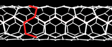
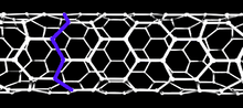
A single-wall carbon nanotube can be imagined as graphene sheet rolled at a certain "chiral" angle with respect to a plane perpendicular to the tube's long axis. Consequently, SWCNT can be defined by its diameter and chiral angle. The chiral angle can range from 0 to 30 degrees.
However, more conveniently, a pair of indices (n, m) is used instead. The indices refer to equally long unit vectors at 60° angles to each other across a single 6-member carbon ring. Taking the origin as carbon number 1, the a1 unit vector may be considered the line drawn from carbon 1 to carbon 3, and the a2 unit vector is then the line drawn from carbon 1 to carbon 5. (See the upper right corner of the diagram at right.) To visualize a CNT with indices (n, m), draw n a1 unit vectors across the graphene sheet, then draw m a2 unit vectors at a 60° angle to the a1 vectors, then add the vectors together. The line representing the sum of the vectors will define the circumference of the CNT along the plane perpendicular to its long axis, connecting one end to the other.[8][9][10] In the diagram at right, Ch is a (4, 2) vector: the sum of 4 unit vectors from the origin directly to the right, then 2 unit vectors at a 60° angle down and to the right.
Tubes having n = m (chiral angle = 30°) are called "armchair" and those with m = 0 (chiral angle = 0°) "zigzag". Those indices uniquely determine whether CNT is a metal, semimetal or semiconductor, as well as its band gap: when |m – n| = 3k (k is integer), the tube is metallic; but if |m – n| = 3k ± 1, the tube is semiconducting. The nanotube diameter d is related to m and n as

In this equation, a = 0.246 nm is the magnitude of either unit vector a1 or a2.
The situation in multi-wall CNTs is complicated as their properties are determined by contribution of all individual shells; those shells have different structures, and, because of the synthesis, are usually more defective than SWCNTs. Therefore, optical properties of MWCNTs will not be considered here.
Van Hove singularities
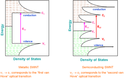

Optical properties of carbon nanotubes derive from electronic transitions within one-dimensional density of states (DOS). A typical feature of one-dimensional crystals is that their DOS is not a continuous function of energy, but it descends gradually and then increases in a discontinuous spike. In contrast, three-dimensional materials have continuous DOS. The sharp peaks found in one-dimensional materials are called Van Hove singularities.
Van Hove singularities result in the following remarkable optical properties of carbon nanotubes:
- Optical transitions occur between the v1 − c1, v2 − c2, etc., states of semiconducting or metallic nanotubes and are traditionally labeled as S11, S22, M11, etc., or, if the "conductivity" of the tube is unknown or unimportant, as E11, E22, etc. Crossover transitions c1 − v2, c2 − v1, etc., are dipole-forbidden and thus are extremely weak, but they were possibly observed using cross-polarized optical geometry.[11]
- The energies between the Van Hove singularities depend on the nanotube structure. Thus by varying this structure, one can tune the optoelectronic properties of carbon nanotube. Such fine tuning has been experimentally demonstrated using UV illumination of polymer-dispersed CNTs.[12]
- Optical transitions are rather sharp (~10 meV) and strong. Consequently, it is relatively easy to selectively excite nanotubes having certain (n, m) indices, as well as to detect optical signals from individual nanotubes.
Kataura plot

The band structure of carbon nanotubes having certain (n, m) indexes can be easily calculated.[13] A theoretical graph based on this calculations was designed in 1999 by Hiromichi Kataura to rationalize experimental findings. A Kataura plot relates the nanotube diameter and its bandgap energies for all nanotubes in a diameter range.[14] The oscillating shape of every branch of the Kataura plot reflects the intrinsic strong dependence of the SWCNT properties on the (n, m) index rather than on its diameter. For example, (10, 1) and (8, 3) tubes have almost the same diameter, but very different properties: the former is a metal, but the latter is a semiconductor.
Optical absorption

Optical absorption in carbon nanotubes differs from absorption in conventional 3D materials by presence of sharp peaks (1D nanotubes) instead of an absorption threshold followed by an absorption increase (most 3D solids). Absorption in nanotubes originates from electronic transitions from the v2 to c2 (energy E22) or v1 to c1 (E11) levels, etc.[8][14] The transitions are relatively sharp and can be used to identify nanotube types. Note that the sharpness deteriorates with increasing energy, and that many nanotubes have very similar E22 or E11 energies, and thus significant overlap occurs in absorption spectra. This overlap is avoided in photoluminescence mapping measurements (see below), which instead of a combination of overlapped transitions identifies individual (E22, E11) pairs.[15][16]
Interactions between nanotubes, such as bundling, broaden optical lines. While bundling strongly affects photoluminescence, it has much weaker effect on optical absorption and Raman scattering. Consequently, sample preparation for the latter two techniques is relatively simple.
Optical absorption is routinely used to quantify quality of the carbon nanotube powders.[17]
The spectrum is analyzed in terms of intensities of nanotube-related peaks, background and pi-carbon peak; the latter two mostly originate from non-nanotube carbon in contaminated samples. However, it has been recently shown that by aggregating nearly single chirality semiconducting nanotubes into closely packed Van der Waals bundles the absorption background can be attributed to free carrier transition originating from intertube charge transfer.[18]
Carbon nanotubes as a black body
An ideal black body should have emissivity or absorbance of 1.0, which is difficult to attain in practice, especially in a wide spectral range. Vertically aligned "forests" of single-wall carbon nanotubes can have absorbances of 0.98–0.99 from the far-ultraviolet (200 nm) to far-infrared (200 μm) wavelengths.
These SWNT forests (buckypaper) were grown by the super-growth CVD method to about 10 μm height. Two factors could contribute to strong light absorption by these structures: (i) a distribution of CNT chiralities resulted in various bandgaps for individual CNTs. Thus a compound material was formed with broadband absorption. (ii) Light might be trapped in those forests due to multiple reflections.[19][20][21]
| UV-to-near IR | Near-to-mid IR | Mid-to-far IR | |
|---|---|---|---|
| Wavelength, μm | 0.2-2 | 2–20 | 25–200 |
| Incident angle, ° | 8 | 5 | 10 |
| Reflection | Hemispherical-directional | Hemispherical-directional | Specular |
| Reference | White reflectance standard | Gold mirror | Aluminum mirror |
| Average reflectance | 0.0160 | 0.0097 | 0.0017 |
| Standard deviation | 0.0048 | 0.0041 | 0.0027 |
Luminescence

Photoluminescence (Fluorescence)
Semiconducting single-walled carbon nanotubes emit near-infrared light upon photoexcitation, described interchangeably as fluorescence or photoluminescence (PL). The excitation of PL usually occurs as follows: an electron in a nanotube absorbs excitation light via S22 transition, creating an electron-hole pair (exciton). Both electron and hole rapidly relax (via phonon-assisted processes) from c2 to c1 and from v2 to v1 states, respectively. Then they recombine through a c1 − v1 transition resulting in light emission.
No excitonic luminescence can be produced in metallic tubes. Their electrons can be excited, thus resulting in optical absorption, but the holes are immediately filled by other electrons out of the many available in the metal. Therefore, no excitons are produced.
Salient properties
- Photoluminescence from SWCNT, as well as optical absorption and Raman scattering, is linearly polarized along the tube axis. This allows monitoring of the SWCNTs orientation without direct microscopic observation.
- PL is quick: relaxation typically occurs within 100 picoseconds.[23]
- PL efficiency was first found to be low (~0.01%),[23] but later studies measured much higher quantum yields. By improving the structural quality and isolation of nanotubes, emission efficiency increased. A quantum yield of 1% was reported in nanotubes sorted by diameter and length through gradient centrifugation,[24] and it was further increased to 20% by optimizing the procedure of isolating individual nanotubes in solution.[25]
- The spectral range of PL is rather wide. Emission wavelength can vary between 0.8 and 2.1 micrometers depending on the nanotube structure.[15][16]
- Excitons are apparently delocalized over several nanotubes in single chirality bundles as the photoluminescence spectrum displays a splitting consistent with intertube exciton tunneling.[18]
- Interaction between nanotubes or between a nanotube and another material may quench or increase PL.[26] No PL is observed in multi-walled carbon nanotubes. PL from double-wall carbon nanotubes strongly depends on the preparation method: CVD grown DWCNTs show emission both from inner and outer shells.[15][16] However, DWCNTs produced by encapsulating fullerenes into SWCNTs and annealing show PL only from the outer shells.[27] Isolated SWCNTs lying on the substrate show extremely weak PL which has been detected in few studies only.[28] Detachment of the tubes from the substrate drastically increases PL.
- Position of the (S22, S11) PL peaks depends slightly (within 2%) on the nanotube environment (air, dispersant, etc.). However, the shift depends on the (n, m) index, and thus the whole PL map not only shifts, but also warps upon changing the CNT medium.
Applications
- Photoluminescence is used for characterization purposes to measure the quantities of semiconducting nanotube species in a sample. Nanotubes are isolated (dispersed) using an appropriate chemical agent ("dispersant") to reduce the intertube quenching. Then PL is measured, scanning both the excitation and emission energies and thereby producing a PL map. The ovals in the map define (S22, S11) pairs, which unique identify (n, m) index of a tube. The data of Weisman and Bachilo are conventionally used for the identification.[29]
- Nanotube fluorescence has been investigated for the purposes of imaging and sensing in biomedical applications.[30][31][32]
Sensitization
Optical properties, including the PL efficiency, can be modified by encapsulating organic dyes (carotene, lycopene, etc.) inside the tubes.[33][34] Efficient energy transfer occurs between the encapsulated dye and nanotube — light is efficiently absorbed by the dye and without significant loss is transferred to the SWCNT. Thus potentially, optical properties of a carbon nanotube can be controlled by encapsulating certain molecule inside it. Besides, encapsulation allows isolation and characterization of organic molecules which are unstable under ambient conditions. For example, Raman spectra are extremely difficult to measure from dyes because of their strong PL (efficiency close to 100%). However, encapsulation of dye molecules inside SWCNTs completely quenches dye PL, thus allowing measurement and analysis of their Raman spectra.[35]
Cathodoluminescence
Cathodoluminescence (CL) — light emission excited by electron beam — is a process commonly observed in TV screens. An electron beam can be finely focused and scanned across the studied material. This technique is widely used to study defects in semiconductors and nanostructures with nanometer-scale spatial resolution.[36] It would be beneficial to apply this technique to carbon nanotubes. However, no reliable CL, i.e. sharp peaks assignable to certain (n, m) indices, has been detected from carbon nanotubes yet.
Electroluminescence
If appropriate electrical contacts are attached to a nanotube, electron-hole pairs (excitons) can be generated by injecting electrons and holes from the contacts. Subsequent exciton recombination results in electroluminescence (EL). Electroluminescent devices have been produced from single nanotubes[3][4][37] and their macroscopic assemblies.[38] Recombination appears to proceed via triplet-triplet annihilation[39] giving distinct peaks corresponding to E11 and E22 transitions.[38]
Raman scattering

Raman spectroscopy has good spatial resolution (~0.5 micrometers) and sensitivity (single nanotubes); it requires only minimal sample preparation and is rather informative. Consequently, Raman spectroscopy is probably the most popular technique of carbon nanotube characterization. Raman scattering in SWCNTs is resonant, i.e., only those tubes are probed which have one of the bandgaps equal to the exciting laser energy.[40][41] Several scattering modes dominate the SWCNT spectrum, as discussed below.
Similar to photoluminescence mapping, the energy of the excitation light can be scanned in Raman measurements, thus producing Raman maps.[40] Those maps also contain oval-shaped features uniquely identifying (n, m) indices. Contrary to PL, Raman mapping detects not only semiconducting but also metallic tubes, and it is less sensitive to nanotube bundling than PL. However, requirement of a tunable laser and a dedicated spectrometer is a strong technical impediment.
Radial breathing mode
Radial breathing mode (RBM) corresponds to radial expansion-contraction of the nanotube. Therefore, its frequency νRBM (in cm−1) depends on the nanotube diameter d as, νRBM= A/d + B (where A and B are constants dependent on the environment in which the nanotube is present. For example, B=0 for individual nanotubes.) (in nanometers) and can be estimated[40][41] as νRBM = 234/d + 10 for SWNT or νRBM = 248/d for DWNT, which is very useful in deducing the CNT diameter from the RBM position. Typical RBM range is 100–350 cm−1. If RBM intensity is particularly strong, its weak second overtone can be observed at double frequency.
Bundling mode
The bundling mode is a special form of RBM supposedly originating from collective vibration in a bundle of SWCNTs.[42]
G mode
Another very important mode is the G mode (G from graphite). This mode corresponds to planar vibrations of carbon atoms and is present in most graphite-like materials.[10] G band in SWCNT is shifted to lower frequencies relative to graphite (1580 cm−1) and is split into several peaks. The splitting pattern and intensity depend on the tube structure and excitation energy; they can be used, though with much lower accuracy compared to RBM mode, to estimate the tube diameter and whether the tube is metallic or semiconducting.
D mode
D mode is present in all graphite-like carbons and originates from structural defects.[10] Therefore, the ratio of the G/D modes is conventionally used to quantify the structural quality of carbon nanotubes. High-quality nanotubes have this ratio significantly higher than 100. At a lower functionalisation of the nanotube, the G/D ratio remains almost unchanged. This ratio gives an idea of the functionalisation of a nanotube.
G' mode
The name of this mode is misleading: it is given because in graphite, this mode is usually the second strongest after the G mode. However, it is actually the second overtone of the defect-induced D mode (and thus should logically be named D'). Its intensity is stronger than that of the D mode due to different selection rules.[10] In particular, D mode is forbidden in the ideal nanotube and requires a structural defect, providing a phonon of certain angular momentum, to be induced. In contrast, G' mode involves a "self-annihilating" pair of phonons and thus does not require defects. The spectral position of G' mode depends on diameter, so it can be used roughly to estimate the SWCNT diameter.[16] In particular, G' mode is a doublet in double-wall carbon nanotubes, but the doublet is often unresolved due to line broadening.
Other overtones, such as a combination of RBM+G mode at ~1750 cm−1, are frequently seen in CNT Raman spectra. However, they are less important and are not considered here.
Anti-Stokes scattering
All the above Raman modes can be observed both as Stokes and anti-Stokes scattering. As mentioned above, Raman scattering from CNTs is resonant in nature, i.e. only tubes whose band gap energy is similar to the laser energy are excited. The difference between those two energies, and thus the band gap of individual tubes, can be estimated from the intensity ratio of the Stokes/anti-Stokes lines.[40][41] This estimate however relies on the temperature factor (Boltzmann factor), which is often miscalculated – a focused laser beam is used in the measurement, which can locally heat the nanotubes without changing the overall temperature of the studied sample.
Rayleigh scattering
Carbon nanotubes have very large aspect ratio, i.e., their length is much larger than their diameter. Consequently, as expected from the classical electromagnetic theory, elastic light scattering (or Rayleigh scattering) by straight CNTs has anisotropic angular dependence, and from its spectrum, the band gaps of individual nanotubes can be deduced.[43][44]
Another manifestation of Rayleigh scattering is the "antenna effect", an array of nanotubes standing on a substrate has specific angular and spectral distributions of reflected light, and both those distributions depend on the nanotube length.[45]
See also
- Allotropes of carbon
- Buckypaper
- Carbon nanotube
- Carbon nanotubes in photovoltaics
- Graphene
- Hiromichi Kataura
- Mechanical properties of carbon nanotubes
- Nanoflower
- Potential applications of carbon nanotubes
- Resonance Raman spectroscopy
- Selective chemistry of single-walled nanotubes
- Vantablack, a substance produced in 2014; the blackest substance known
References
- ↑ Zhang, R.; Zhang, Y.; Zhang, Q.; Xie, H.; Qian, W.; Wei, F. (2013). "Growth of Half-Meter Long Carbon Nanotubes Based on Schulz–Flory Distribution". ACS Nano. 7 (7): 6156–61. doi:10.1021/nn401995z. PMID 23806050.
- ↑ Xueshen Wang; et al. (2009). "Fabrication of Ultralong and Electrically Uniform Single-Walled Carbon Nanotubes on Clean Substrates". Nano Letters. 9 (9): 3137–41. Bibcode:2009NanoL...9.3137W. doi:10.1021/nl901260b. PMID 19650638.
- 1 2 J. A. Misewich; et al. (2003). "Electrically Induced Optical Emission from a Carbon Nanotube FET". Science. 300 (5620): 783–786. Bibcode:2003Sci...300..783M. doi:10.1126/science.1081294. PMID 12730598.
- 1 2 J. Chen; et al. (2005). "Bright Infrared Emission from Electrically Induced Excitons in Carbon Nanotubes". Science. 310 (5751): 1171–1174. Bibcode:2005Sci...310.1171C. doi:10.1126/science.1119177. PMID 16293757.
- ↑ M. Freitag; et al. (2003). "Photoconductivity of Single Carbon Nanotubes". Nano Letters. 3 (8): 1067–1071. Bibcode:2003NanoL...3.1067F. doi:10.1021/nl034313e.
- ↑ M. E. Itkis; et al. (2006). "Bolometric Infrared Photoresponse of Suspended Single-Walled Carbon Nanotube Films". Science. 312 (5772): 413–416. Bibcode:2006Sci...312..413I. doi:10.1126/science.1125695. PMID 16627739.
- ↑ A. Star; et al. (2004). "Nanotube Optoelectronic Memory Devices". Nano Letters. 4 (9): 1587–1591. Bibcode:2004NanoL...4.1587S. doi:10.1021/nl049337f.
- 1 2 3 4 S. B. Sinnott & R. Andreys (2001). "Carbon Nanotubes: Synthesis, Properties, and Applications". Critical Reviews in Solid State and Materials Sciences. 26 (3): 145–249. Bibcode:2001CRSSM..26..145S. doi:10.1080/20014091104189.
- 1 2 M. S. Dresselhaus; et al. (1995). "Physics of Carbon Nanotubes". Carbon. 33 (7): 883–891. doi:10.1016/0008-6223(95)00017-8.
- 1 2 3 4 P. C. Eklund; et al. (1995). "Vibrational Modes of Carbon Nanotubes; Spectroscopy and Theory". Carbon. 33 (7): 959–972. doi:10.1016/0008-6223(95)00035-C.
- ↑ Y. Miyauchi; et al. (2006). "Cross-Polarized Optical Absorption of Single-Walled Nanotubes Probed by Polarized Photoluminescence Excitation Spectroscopy". Physical Review B. 74 (20): 205440. arXiv:cond-mat/0608073
 . Bibcode:2006PhRvB..74t5440M. doi:10.1103/PhysRevB.74.205440.
 - ↑ K. Iakoubovskii; et al. (2006). "Midgap Luminescence Centers in Single-Wall Carbon Nanotubes Created by Ultraviolet Illumination" (PDF). Applied Physics Letters. 89 (17): 173108. Bibcode:2006ApPhL..89q3108I. doi:10.1063/1.2364157.
- ↑ S. Maruyama. "Shigeo Maruyama's Fullerene and Carbon Nanotube Site". Retrieved 2008-12-08.
- 1 2 H. Kataura; et al. (1999). "Optical Properties of Single-Wall Carbon Nanotubes" (PDF). Synthetic Metals. 103 (1–3): 2555–2558. doi:10.1016/S0379-6779(98)00278-1.
- 1 2 3 K. Iakoubovskii; et al. (2006). "IR-Extended Photoluminescence Mapping of Single-Wall and Double-Wall Carbon Nanotubes" (PDF). Journal of Physical Chemistry B. 110 (35): 17420–17424. doi:10.1021/jp062653t. PMID 16942079.
- 1 2 3 4 K. Iakoubovskii; et al. (2008). "Optical Characterization of Double-wall Carbon Nanotubes: Evidence for Inner Tube Shielding" (PDF). Journal of Physical Chemistry C. 112 (30): 11194–11198. doi:10.1021/jp8018414.
- ↑ M. E. Itkis; et al. (2005). "Comparison of Analytical Techniques for Purity Evaluation of Single-Walled Carbon Nanotubes". Journal of the American Chemical Society. 127 (10): 3439–48. doi:10.1021/ja043061w. PMID 15755163.
- 1 2 Jared J. Crochet; et al. (2011). "Electrodynamic and Excitonic Intertube Interactions in Semiconducting Carbon Nanotube Aggregates". ACS Nano. 5 (4): 2611–2618. doi:10.1021/nn200427r.
- ↑ Zu-Po Yang; et al. (2008). "Experimental Observation of an Extremely Dark Material Made By a Low-Density Nanotube Array". Nano letters. 8 (2): 446–451. Bibcode:2008NanoL...8..446Y. doi:10.1021/nl072369t. PMID 18181658.
- ↑ K. Mizuno; et al. (2009). "A black body absorber from vertically aligned single-walled carbon nanotubes". Proceedings of the National Academy of Sciences. 106 (15): 6044–6077. Bibcode:2009PNAS..106.6044M. doi:10.1073/pnas.0900155106. PMC 2669394. PMID 19339498.
- ↑ K. Hata; et al. (2004). "Water-Assisted Highly Efficient Synthesis of Impurity-Free Single-Walled Carbon Nanotubes" (PDF). Science. 306 (5700): 1362–1364. Bibcode:2004Sci...306.1362H. doi:10.1126/science.1104962. PMID 15550668.
- ↑ L. Mizuno; et al. (2009). "Supporting Information". Proceedings of the National Academy of Sciences. 106 (15): 6044–7. Bibcode:2009PNAS..106.6044M. doi:10.1073/pnas.0900155106. PMC 2669394. PMID 19339498.
- 1 2 F. Wang; et al. (2004). "Time-Resolved Fluorescence of Carbon Nanotubes and Its Implication for Radiative Lifetimes". Physical Review Letters. 92 (17): 177401. Bibcode:2004PhRvL..92q7401W. doi:10.1103/PhysRevLett.92.177401. PMID 15169189.
- ↑ Jared Crochet; et al. (2007). "Quantum Yield Heterogeneities of Aqueous Single-Wall Carbon Nanotube Suspensions". Journal of the American Chemical Society. 129 (26): 8058–805. doi:10.1021/ja071553d. PMID 17552526.
- ↑ S-Y Ju; et al. (2009). "Brightly Fluorescent Single-Walled Carbon Nanotubes via an Oxygen-Excluding Surfactant Organization". Science. 323 (5919): 1319–1323. Bibcode:2009Sci...323.1319J. doi:10.1126/science.1166265. PMID 19265015.
- ↑ B. C. Satishkumar; et al. (2007). "Reversible fluorescence quenching in carbon nanotubes for biomolecular sensing". Nature Nanotechnology. 2 (9): 560–564. Bibcode:2007NatNa...2..560S. doi:10.1038/nnano.2007.261. PMID 18654368.
- ↑ T. Okazaki; et al. (2006). "Photoluminescence Quenching in Peapod-Derived Double-Walled Carbon Nanotubes" (PDF). Physical Review B. 74 (15): 153404. Bibcode:2006PhRvB..74o3404O. doi:10.1103/PhysRevB.74.153404.
- ↑ N. Ishigami; et al. (2008). "Crystal Plane Dependent Growth of Aligned Single-Walled Carbon Nanotubes on Sapphire". Journal of the American Chemical Society. 130 (30): 9918–9924. doi:10.1021/ja8024752. PMID 18597459.
- ↑ R. B. Weisman & S. M. Bachilo (2003). "Dependence of Optical Transition Energies on Structure for Single-Walled Carbon Nanotubes in Aqueous Suspension: An Empirical Kataura Plot". Nano Letters. 3 (9): 1235–1238. Bibcode:2003NanoL...3.1235W. doi:10.1021/nl034428i.
- ↑ Paul Cherukuri; Sergei M. Bachilo; Silvio H. Litovsky & R. Bruce Weisman (2004). "Near-Infrared Fluorescence Microscopy of Single-Walled Carbon Nanotubes in Phagocytic Cells". Journal of the American Chemical Society. 126: 15638–15639. doi:10.1021/ja0466311.
- ↑ Kevin Welsher; Sarah P. Sherlock & Hongjie Dai (2011). "Deep-tissue anatomical imaging of mice using carbon nanotube fluorophores in the second near-infrared window". Proceedings of the National Academy of Sciences. 108 (22): 8943–8948. arXiv:1105.3536. Bibcode:2011PNAS..108.8943W. doi:10.1073/pnas.1014501108.
- ↑ Paul W. Barone; Seunghyun Baik; Daniel A. Heller & Michael S. Strano (2005). "Near-infrared optical sensors based on single-walled carbon nanotubes". Nature Materials. 4: 86–92. Bibcode:2005NatMa...4...86B. doi:10.1038/nmat1276.
- ↑ K. Yanagi; et al. (2006). "Light-Harvesting Function of β-Carotene Inside Carbon Nanotubes" (PDF). Physical Review B. 74 (15): 155420. Bibcode:2006PhRvB..74o5420Y. doi:10.1103/PhysRevB.74.155420.
- ↑ K. Yanagi; et al. (2007). "Photosensitive Function of Encapsulated Dye in Carbon Nanotubes" (PDF). Journal of the American Chemical Society. 129 (16): 4992–4997. doi:10.1021/ja067351j. PMID 17402730.
- ↑ Y. Saito; et al. (2006). "Vibrational Analysis of Organic Molecules Encapsulated in Carbon Nanotubes by Tip-Enhanced Raman Spectroscopy". Japanese Journal of Applied Physics. 45 (12): 9286–9289. Bibcode:2006JaJAP..45.9286S. doi:10.1143/JJAP.45.9286.
- ↑ S. J. Pennycook; et al. (1980). "Observation of Cathodoluminescence at Single Dislocations by STEM". Philosophical Magazine A. 41 (4): 589–600. Bibcode:1980PMagA..41..589P. doi:10.1080/01418618008239335.
- ↑ M. Freitag; et al. (2004). "Hot Carrier Electroluminescence from a Single Carbon Nanotube". Nano Letters. 4 (6): 1063–1066. Bibcode:2004NanoL...4.1063F. doi:10.1021/nl049607u.
- 1 2 D. Janas; et al. (2013). "Electroluminescence from carbon nanotube films resistively heated in air". Applied Physics Letters. 102 (18): 181104. Bibcode:2013ApPhL.102r1104J. doi:10.1063/1.4804296.
- ↑ D. Janas; et al. (2014). "Direct evidence of delayed electroluminescence from carbon nanotubes on the macroscale". Applied Physics Letters. 104 (26): 261107. Bibcode:2014ApPhL.104z1107J. doi:10.1063/1.4886800.
- 1 2 3 4 C. Fantini; et al. (2004). "Optical Transition Energies for Carbon Nanotubes from Resonant Raman Spectroscopy: Environment and Temperature Effects". Physical Review Letters. 93 (14): 147406. Bibcode:2004PhRvL..93n7406F. doi:10.1103/PhysRevLett.93.147406. PMID 15524844.
- 1 2 3 A. G. Souza Filho; et al. (2004). "Stokes and Anti-Stokes Raman Spectra of Small-Diameter Isolated Carbon Nanotubes". Physical Review B. 69 (11): 115428. Bibcode:2004PhRvB..69k5428S. doi:10.1103/PhysRevB.69.115428.
- ↑ H. Kataura; et al. (2000). "Bundle Effects of Single-Wall Carbon Nanotubes" (PDF). AIP Conference Proceedings. 544. p. 262.
- ↑ M. Y. Sfeir; et al. (2004). "Probing Electronic Transitions in Individual Carbon Nanotubes by Rayleigh Scattering". Science. 306 (5701): 1540–1543. Bibcode:2004Sci...306.1540S. doi:10.1126/science.1103294. PMID 15514117.
- ↑ Y. Wu; et al. (2007). "Variable Electron-Phonon Coupling in Isolated Metallic Carbon Nanotubes Observed by Raman Scattering". Physical Review Letters. 99 (2): 027402. arXiv:0705.3986. Bibcode:2007PhRvL..99b7402W. doi:10.1103/PhysRevLett.99.027402. PMID 17678258.
- ↑ Y. Wang; et al. (2004). "Receiving and Transmitting Light-Like Radio Waves: Antenna Effect in Arrays of Aligned Carbon Nanotubes". Applied Physics Letters. 85 (13): 2607. Bibcode:2004ApPhL..85.2607W. doi:10.1063/1.1797559.
External links
- Selection of free-download articles on carbon nanotubes (New Journal of Physics)
- Publications of H. Kataura — many of older ones are downloadable
- Carbon Nanotube Black Body (AIST nano tech 2009)