OpenRISC 1200

The OpenRISC 1200 (OR1200) is an implementation of the open source OpenRISC 1000 RISC architecture .
A synthesizable CPU core, it was for many years maintained by developers at OpenCores.org, although, since 2015, that activity has now been taken over by the Free and Open Source Silicon Foundation at the librecores.org website. The Verilog RTL description is released under the GNU Lesser General Public License (LGPL).
Architecture
The IP core of the OR1200 is implemented in the Verilog HDL. As an open source core, the design is fully public and may be downloaded and modified by any individual. The official implementation is maintained by developers at OpenCores.org. The implementation specifies a power management unit, debug unit, tick timer, programmable interrupt controller (PIC), central processing unit (CPU), and memory management hardware. Peripheral systems and a memory subsystem may be added using the processor's implementation of a standardized 32-bit Wishbone bus interface. The OR1200 is intended to have a performance comparable to an ARM10 processor architecture.
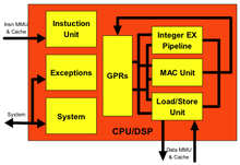
CPU/DSP
The OR1200 CPU is an implementation of the 32-bit ORBIS32 instruction set architecture (ISA) and (optionally) ORFP32X ISA implementing IEEE-754 compliant single precision floating point support. The ISA has five instruction formats and supports two addressing modes: register indirect with displacement, and PC-relative. The implementation has a single-issue 5-stage pipeline and is capable of single cycle execution on most instructions. The CPU also contains a MAC unit in order to better support digital signal processing (DSP) applications.
Memory Management
The OR1200 design uses a Harvard memory architecture and therefore has separate memory management units (MMUs) for data and instruction memories. These MMUs each consist of a hash-based 1-way direct-mapped translation lookaside buffer (TLB) with page size of 8 KB and a default size of 64 entries. The TLBs are individually scalable from 16 to 256 entries. There is also a one-way direct-mapped cache each for both the instruction memory and for the data memory. Each cache has a default size of 8 KB, but both are individually scalable between 1 and 64 KB. The MMU includes support for virtual memory.
Performance
The core achieves 1.34 CoreMarks per MHz at 50 MHz on Xilinx FPGA technology.
Under the worst case, the clock frequency for the OR1200 is 250 MHz at a 0.18 µm 6LM fabrication process. Using the Dhrystone benchmark, a 250 MHz OR1200 processor performs 250 Dhrystone millions of instructions per second (DMIPS) in the worst case. Estimated power usage of a 250 MHz processor at a .18 µm process is less than 1W at full throttle and less than 5 mW at half throttle.
Applications
Generally, the OR1200 is intended to be used in a variety of embedded applications, including telecommunications, portable media, home entertainment, and automotive applications. The GNU toolchain (including GCC) has also been successfully ported to the architecture, although it is not bug-free . There is a port of the Linux kernel for OR1K which runs on the OR1200. Recent ports of the embedded C libraries newlib and uClibc are also available for the platform.
Implementations
The OR1200 has been successfully implemented using FPGA and ASIC technologies.[1]
History
The first public record of the OpenRISC 1000 architecture is in 2000..
References
- ↑ ?
- ORSoC.se "OpenRISC 1200 development board". March 2009
- Cragie, Robert. "OpenRISC Resources Page." Asisi. March 19, 2008.
External links
- OR1200 page at OpenCores.org
- OR1200 specification at OpenCores.org (warning: URL serves context-type text/plain for PDF data)