Metal–semiconductor junction
In solid-state physics, a metal–semiconductor (M–S) junction is a type of junction in which a metal comes in close contact with a semiconductor material. It is the oldest practical semiconductor device. M–S junctions can either be rectifying or non-rectifying. The rectifying metal–semiconductor junction forms a Schottky barrier, making a device known as a Schottky diode, while the non-rectifying junction is called an ohmic contact.[1] (In contrast, a rectifying semiconductor–semiconductor junction, the most common semiconductor device today, is known as a p–n junction.)
Metal–semiconductor junctions are crucial to the operation of all semiconductor devices. Usually an ohmic contact is desired, so that electrical charge can be conducted easily between the active region of a transistor and the external circuitry. Occasionally however a Schottky barrier is useful, as in Schottky diodes, Schottky transistors, and metal–semiconductor field effect transistors.
The critical parameter: Schottky barrier height
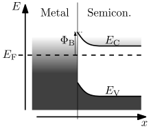
Whether a given metal-semiconductor junction is an ohmic contact, or Schottky barrier, depends on the Schottky barrier height, ΦB, of the junction. For a sufficiently large Schottky barrier height, where ΦB is significantly higher than the thermal energy kT, the semiconductor is depleted near the metal and behaves as a Schottky barrier. For lower Schottky barrier heights, the semiconductor is not depleted and instead forms an ohmic contact to the metal.
The Schottky barrier height is defined differently for n-type and p-type semiconductors (being measured from the conduction band edge and valence band edge, respectively). The alignment of the semiconductor's bands near the junction is typically independent of the semiconductor's doping level, so the n-type and p-type Schottky barrier heights are ideally related to each other by:

where Eg is the semiconductor's band gap.
In practice, the Schottky barrier height is not precisely constant across the interface, and varies over the interfacial surface.[2]
Schottky–Mott rule and Fermi level pinning


The Schottky–Mott rule of Schottky barrier formation predicts the Schottky barrier height based on the vacuum work function of the metal relative to the vacuum electron affinity (or vacuum ionization energy) of the semiconductor:

This model is derived based on the thought experiment of bringing together the two materials in vacuum, and is closely related in logic to Anderson's rule for semiconductor-semiconductor junctions. Different semiconductors respect the Schottky–Mott rule to varying degrees.[5]
Although the Schottky–Mott model correctly predicted the existence of band bending in the semiconductor, it was found experimentally that it would give grossly incorrect predictions for the height of the Schottky barrier. A phenomenon referred to as "Fermi level pinning" caused some point of the band gap, at which DOS exists, to be locked (pinned) to the Fermi level. This made the Schottky barrier height almost completely insensitive to the metal's work function:[5]

where Ebandgap is the size of band gap in the semiconductor.
It was noted in 1947 by John Bardeen that the Fermi level pinning phenomenon would naturally arise if there were chargeable states in the semiconductor right at the interface, with energies inside the semiconductor's gap. These would either be induced during the direct chemical bonding of the metal and semiconductor (metal-induced gap states) or be already present in the semiconductor–vacuum surface (surface states). These highly dense surface states would be able to absorb a large quantity of charge donated from the metal, effectively shielding the semiconductor from the details of the metal. As a result, the semiconductor's bands would necessarily align to a location relative to the surface states which are in turn pinned to the Fermi level (due to their high density), all without influence from the metal.[4]
The Fermi level pinning effect is strong in many commercially important semiconductors (Si, Ge, GaAs),[5] and thus can be very frustrating for the design of semiconductor devices. For example, nearly all metals form a significant Schottky barrier to n-type germanium and an ohmic contact to p-type germanium, since the valence band edge is strongly pinned to the metal's Fermi level.[6] The solution to this inflexibility requires additional processing steps such as adding an intermediate insulating layer to unpin the bands. (In the case of germanium, germanium nitride has been used[7])
History
The rectification property of metal–semiconductor contacts was discovered by Ferdinand Braun in 1874 using mercury metal contacted with copper and iron sulfide semiconductors.[8]
G.W. Pickard received a patent in 1906 on a point-contact rectifier using silicon. In 1907, George W. Pierce published a paper in Physical Review showing rectification properties of diodes made by sputtering many metals on many semiconductors.[9] The use of the metal–semiconductor diode rectifier was proposed by Lilienfeld in 1926 in the first of his three transistor patents as the gate of the metal–semiconductor field effect transistors.[10] The correct theory of the field-effect transistor using a metal/semiconductor gate was advanced by William Shockley in 1939.
The earliest metal–semiconductor diodes in electronics application occurred around 1900, when the cat's whisker rectifiers were used in receivers.[11] They consisted of pointed tungsten wire (in the shape of a cat's whisker) whose tip or point was pressed against the surface of a galena (lead sulfide) crystal. The first large area rectifier appeared around 1926 which consisted of a copper(I) oxide semiconductor thermally grown on a copper substrate. Subsequently, selenium films were evaporated onto large metal substrates to form the rectifying diodes. These selenium rectifiers were used (and are still used) to convert alternating current to direct current in electrical power applications. During 1925–1940, diodes consisting of a pointed tungsten metal wire in contact with a silicon crystal base, were fabricated in laboratories to detect microwaves in the UHF range. A World War II program to manufacture high-purity silicon as the crystal base for the point-contact rectifier was suggested by Frederick Seitz in 1942 and successfully undertaken by the Experimental Station of the E. I du Pont de Nemours Company.
The first theory that predicted the correct direction of rectification of the metal–semiconductor junction was given by Nevill Mott in 1939. He found the solution for both the diffusion and drift currents of the majority carriers through the semiconductor surface space charge layer which has been known since about 1948 as the Mott barrier. Walter H. Schottky and Spenke extended Mott's theory by including a donor ion whose density is spatially constant through the semiconductor surface layer. This changed the constant electric field assumed by Mott to a linearly decaying electric field. This semiconductor space-charge layer under the metal is known as the Schottky barrier. A similar theory was also proposed by Davydov in 1939. Although it gives the correct direction of rectification, it has also been proven that the Mott theory and its Schottky-Davydov extension gives the wrong current limiting mechanism and wrong current-voltage formulae in silicon metal/semiconductor diode rectifiers. The correct theory was developed by Hans Bethe and reported by him in a M.I.T. Radiation Laboratory Report dated November 23, 1942. In Bethe's theory, the current is limited by thermionic emission of electrons over the metal–semiconductor potential barrier. Thus, the appropriate name for the metal–semiconductor diode should be the Bethe diode, instead of the Schottky diode, since the Schottky theory does not predict the modern metal–semiconductor diode characteristics correctly.[12]
References
- ↑ Semiconductor Devices: Modelling and Technology, Nandita Dasgupta, Amitava Dasgupta.(2004) ISBN 81-203-2398-X.
- ↑ http://academic.brooklyn.cuny.edu/physics/tung/Schottky/inhomo.htm
- ↑ Tung, R. (2001). "Formation of an electric dipole at metal-semiconductor interfaces". Physical Review B. 64 (20). Bibcode:2001PhRvB..64t5310T. doi:10.1103/PhysRevB.64.205310.
- 1 2 Bardeen, J. (1947). "Surface States and Rectification at a Metal Semi-Conductor Contact". Physical Review. 71 (10): 717. Bibcode:1947PhRv...71..717B. doi:10.1103/PhysRev.71.717.
- 1 2 3 http://academic.brooklyn.cuny.edu/physics/tung/Schottky/systematics.htm
- ↑ Nishimura, T.; Kita, K.; Toriumi, A. (2007). "Evidence for strong Fermi-level pinning due to metal-induced gap states at metal/germanium interface". Applied Physics Letters. 91 (12): 123123. Bibcode:2007ApPhL..91l3123N. doi:10.1063/1.2789701.
- ↑ Lieten, R. R.; Degroote, S.; Kuijk, M.; Borghs, G. (2008). "Ohmic contact formation on n-type Ge". Applied Physics Letters. 92 (2): 022106. Bibcode:2008ApPhL..92b2106L. doi:10.1063/1.2831918.
- ↑ Braun, F. (1874), "Ueber die Stromleitung durch Schwefelmetalle" [On current conduction through metal sulfides], Annalen der Physik und Chemie (in German), 153 (4): 556–563, doi:10.1002/andp.18752291207
- ↑ Pierce, G. W. (1907). "Crystal Rectifiers for Electric Currents and Electric Oscillations. Part I. Carborundum". Physical Review (Series I). 25: 31. Bibcode:1907PhRvI..25...31P. doi:10.1103/PhysRevSeriesI.25.31.
- ↑ US 1745175 "Method and apparatus for controlling electric current" first filed in Canada on 22.10.1925.
- ↑ US 755840, Bose, Jagadis Chunder, "Detector for electrical disturbances", published September 30, 1901, issued March 29, 1904
- ↑ Sah, Chih-Tang (1991). Fundamentals of Solid-State Electronics. World Scientific. ISBN 9810206372.