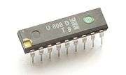
Intel 8008
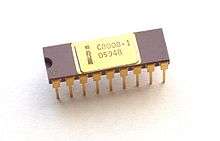 An Intel 8008 | |
| Produced | From mid 1972 to 1983[1] |
|---|---|
| Common manufacturer(s) |
|
| Max. CPU clock rate | 0.2 MHz to 0.8 MHz |
| Min. feature size | 10μm |
| Instruction set | 8008 |
| Predecessor | Intel 4004 |
| Successor | Intel 8080 |
| Application | Computer terminals, calculators, bottling machines, 1970s ASEA industrial robots[2] (IRB 6), simple computers, etc. |
| Package(s) |
|
The Intel 8008 ("eight-thousand-eight" or "eighty-oh-eight") is an early byte-oriented microprocessor designed and manufactured by Intel and introduced in April 1972. It was an 8-bit CPU with an external 14-bit address bus that could address 16 KB of memory. Originally known as the 1201, the chip was commissioned by Computer Terminal Corporation (CTC) to implement an instruction set of their design for their Datapoint 2200 programmable terminal. As the chip was delayed and did not meet CTC's performance goals, the 2200 ended up using CTC's own TTL-based CPU instead. An agreement permitted Intel to market the chip to other customers after Seiko expressed an interest in using it for a calculator.
History
CTC formed in San Antonio in 1968 under the direction of Austin O. "Gus" Roche and Phil Ray, both NASA engineers. Roche, in particular, was primarily interested in producing a desktop computer. However, given the immaturity of the market, the company's business plan mentioned only a Teletype Model 33 ASR replacement, which shipped as the Datapoint 3300. The case was deliberately designed to fit in the same space as an IBM Selectric typewriter, and used a video screen shaped to be the same aspect ratio as an IBM punched card.[3] Although commercially successful, the 3300 had ongoing heat problems due to the amount of circuitry packed into such a small space.
In order to address the heating and other issues, a re-design started that featured the CPU part of the internal circuitry re-implemented on a single chip. Looking for a company able to produce their chip design, Roche turned to Intel, then primarily a vendor of memory chips.[3] Roche met with Bob Noyce, who expressed concern with the concept; John Frassanito recalls that "Noyce said it was an intriguing idea, and that Intel could do it, but it would be a dumb move. He said that if you have a computer chip, you can only sell one chip per computer, while with memory, you can sell hundreds of chips per computer."[3] Another major concern was that Intel's existing customer base purchased their memory chips for use with their own processor designs; if Intel introduced their own processor, they might be seen as a competitor, and their customers might look elsewhere for memory. Nevertheless, Noyce agreed to a $50,000 development contract in early 1970. Texas Instruments (TI) was also brought in as a second supplier.
TI was able to make samples of the 1201 based on Intel drawings, but these proved to be buggy and were rejected. Intel's own versions were delayed. CTC decided to re-implement the new version of the terminal using discrete TTL instead of waiting for a single chip CPU. The new system was released as the Datapoint 2200 in the spring 1970, with their first sale to General Mills on May 25, 1970.[3] CTC paused development of the 1201 after the 2200 was released, as it was no longer needed. Six months later, Seiko approached Intel expressing an interest in using the 1201 in a scientific calculator, likely after seeing the success of the simpler Intel 4004 used by Busicom in their business calculators. A small re-design followed, under the leadership of Federico Faggin, the designer of the 4004, now project leader of the 1201, expanding from a 16-pin to 18-pin design, and the new 1201 was delivered to CTC in late 1971.[3]
By that point CTC had once again moved on, this time to the Datapoint 2200 II, which was faster. The 1201 was no longer powerful enough for the new model. CTC voted to end their involvement with the 1201, leaving the design's intellectual property to Intel instead of paying the $50,000 contract. Intel renamed it the 8008, and put it in their catalog in April 1972 priced at $120. Intel's initial worries about their existing customer base leaving them proved unfounded, and the 8008 went on to be a commercially successful design. This was followed by the Intel 8080, and then the hugely successful Intel x86 family.[3]
One of the first teams to build a complete system around the 8008 was Bill Pentz' team at California State University, Sacramento. The Sac State 8008 was possibly the first true microcomputer, with a disk operating system built with IBM Basic assembly language in PROM all driving a color display, hard drive, keyboard, modem, audio/paper tape reader and printer. The project started in the spring of 1972 and with key help from Tektronix the system was fully functional a year later. Bill assisted Intel with the MCS-8 kit and provided key input to the Intel 8080 instruction set which helped make it useful for the industry and hobbyists.
In the UK, a team at S. E. Laboratories Engineering (EMI) led by Tom Spink in 1972 built a microcomputer based on a pre-release sample of the 8008. Joe Hardman extended the chip with an external stack. This, among other things, gave it power-fail save and recovery. Joe also developed a direct screen printer. The operating system was written using a meta-assembler developed by L. Crawford and J. Parnell for a Digital Equipment Corporation PDP-11.[4] The operating system was burnt into a PROM. It was interrupt-driven, queued, and based on a fixed page size for programs and data. An operational prototype was prepared for management, who decided not to continue with the project.
The 8008 was the CPU for the very first commercial, non-calculator personal computers (excluding the Datapoint 2200 itself): the US SCELBI kit and the pre-built French Micral N and Canadian MCM/70.
Design
| Intel 8008 registers | |||||||||||||||||||||||||||||||||||||||||||||||||||||||||||||||||||||||||||||||||||||||||||||||||||||||||||||||||||||||||||||||||||||||||||||||||||||||||||||||||||||||||||||||||||||||||||||||||||||||||||||||||||||||||||||||||||||||||||||||||||||||||||||||||||||||||||||||||||||||||||||||||||||||||||||||||||||||||||
| |||||||||||||||||||||||||||||||||||||||||||||||||||||||||||||||||||||||||||||||||||||||||||||||||||||||||||||||||||||||||||||||||||||||||||||||||||||||||||||||||||||||||||||||||||||||||||||||||||||||||||||||||||||||||||||||||||||||||||||||||||||||||||||||||||||||||||||||||||||||||||||||||||||||||||||||||||||||||||
Implemented in 10 μm silicon-gate enhancement-mode PMOS; initial versions of the 8008 could work at clock frequencies up to 0.5 MHz, this was later increased in the 8008-1 to a specified maximum of 0.8 MHz. Instructions took between 5 and 11 T-states, where each T-state was 2 clock cycles.[5] Register–register loads and ALU operations took 5T (20 μs at 0.5 MHz), register–memory 8T (32 μs), while calls and jumps (when taken) took 11 T-states (44 μs).[6] The 8008 was a little slower in terms of instructions per second (36,000 to 80,000 at 0.8 MHz) than the 4-bit Intel 4004 and Intel 4040,[7] but the fact that the 8008 processed data 8 bits at a time and could access significantly more RAM still gave it a significant speed advantage in most applications. The 8008 had 3,500 transistors.[8][9][10]
The chip (limited by its 18-pin DIP packaging) had a single 8-bit bus and required a significant amount of external support logic. For example, the 14-bit address, which could access "16 K × 8 bits of memory",[5] needed to be latched by some of this logic into an external Memory Address Register (MAR). The 8008 could access 8 input ports and 24 output ports.
For controller and CRT terminal use, this was an acceptable design, but it was rather cumbersome to use for most other tasks, at least compared to the next generations of microprocessors. A few early computer designs were based on it, but most would use the later and greatly improved Intel 8080 instead.
Related processor designs
The subsequent 40-pin NMOS Intel 8080 expanded upon the 8008 registers and instruction set and implemented a more efficient external bus interface (using the 22 additional pins). Despite a close architectural relationship, the 8080 was not made binary compatible with the 8008, so an 8008 program would not run on an 8080. However, as two different assembly syntaxes were used by Intel at the time, the 8080 could be used in an 8008 assembly-language backward-compatible fashion.[11]
The Intel 8085 was an electrically modernized version of the 8080 that used depletion-mode transistors and also added a few instructions.
The Intel 8086, the original x86 processor, was a non-strict extension of the 8080, so it loosely resembled the original Datapoint 2200 design as well. Almost every Datapoint 2200 and 8008 instruction has an equivalent not only in the instruction set of the 8080, 8085, and Z80, but also in the instruction set of modern x86 processors (although the instruction encodings are different).
Features
- Seven 8-bit "scratchpad" registers: The main accumulator (A) and six other registers (B, C, D, E, H, and L).
- 14-bit program counter (PC).
- Seven-level push-down address call stack. Eight registers are actually used, with the top-most register being the PC.
- Four condition code status flags: carry (C), even parity (P), zero (Z), and sign (S).
- Indirect memory access using the H and L registers (HL) as a 14-bit data pointer (the upper two bits are ignored).
Example code
The following 8008 assembler source code is for a subroutine named MEMCPY that copies a block of data bytes of a given size from one location to another.
                    ; MEMCPY --
                    ; Copy a block of memory from one location to another.
                    ;
                    ; Entry parameters
                    ;       SRC: 14-bit address of source data block
                    ;       DST: 14-bit address of target data block
                    ;       CNT: 14-bit count of bytes to copy

                                ORG     1700Q       ;Data at 001700q
001700  000         SRC         DFB     0           ;SRC, low byte
001701  000                     DFB     0           ;     high byte
001702  000         DST         DFB     0           ;DST, low byte
001703  000                     DFB     0           ;     high byte
001704  000         CNT         DFB     0           ;CNT, low byte
001705  000                     DFB     0           ;     high byte

                                ORG     2000Q       ;Code at 002000q
002000  066 304     MEMCPY      LLI     CNT+0       ;HL = addr(CNT)
002002  056 003                 LHI     CNT+1
002004  327                     LCM                 ;BC = CNT
002005  060                     INL
002006  317                     LBM
002007  302         LOOP        LAC                 ;If BC = 0,
002010  261                     ORB
002011  053                     RTZ                 ;Return
002012  302         DECCNT      LAC                 ;BC = BC-1
002013  024 001                 SUI     1
002015  320                     LCA
002016  301                     LAB
002017  034 000                 SBI     0
002021  310                     LBA
002022  066 300     GETSRC      LLI     SRC+0       ;HL = addr(SRC)
002024  056 003                 LHI     SRC+1
002026  347                     LEM                 ;DE = SRC
002027  060                     INL
002030  337                     LDM
002031  302                     LAC                 ;HL = DE+BC
002032  206                     ADE
002033  360                     LLA
002034  301                     LAB
002035  215                     ACD
002036  350                     LHA
002037  307                     LAM                 ;Load A from (HL)
002040  066 302     GETDST      LLI     DST+0       ;HL = addr(DST)
002042  056 003                 LHI     DST+1
002044  347                     LEM                 ;DE = DST
002045  060                     INL
002046  337                     LDM
002047  364                     LLE                 ;HL = DE
002050  353                     LHD
002051  330                     LDA                 ;D = A
002052  302                     LAC                 ;HL = HL+BC
002053  206                     ADL
002054  360                     LLA
002055  301                     LAB
002056  215                     ACH
002057  350                     LHA
002060  373                     LMD                 ;Store D to (HL)
002061  104 007 004             JMP     LOOP        ;Repeat the loop
002064                          END
In the code above, all values are given in octal. Locations SRC, DST, and CNT are 16-bit parameters for the subroutine named MEMCPY. In actuality, only 14 bits of the values are used, since the CPU has only a 14-bit addressable memory space. The values are stored in little-endian format, although this is an arbitrary choice, since the CPU is incapable of reading or writing more than a single byte into memory at a time. Since there is no instruction to load a register directly from a given memory address, the HL register pair must first be loaded with the address, and the target register can then be loaded from the M operand, which is an indirect load from the memory location in the HL register pair. The BC register pair is loaded with the CNT parameter value, and decremented at the end of the loop until it becomes zero. Note that most of the instructions used occupy a single 8-bit opcode.
Designers
- CTC (Instruction set and architecture): Victor Poor and Harry Pyle.
- Intel (Implementation in silicon):
- Ted Hoff and Stan Mazor and Larry Potter (IBM Chief Scientist of IBM) proposed a single-chip implementation of the CTC architecture, using RAM register memory rather than shift register memory, and also added a few instructions and interrupt facility. The 8008 (originally called 1201) chip design started before the 4004 development. Hoff and Mazor, however, could not and did not develop a "silicon design" because they were neither chip designers nor process developers and furthermore the necessary silicon-gate-based design methodology and circuits, under development by Federico Faggin for the 4004, were not yet available.[12]
- Federico Faggin, having finished the design of the 4004, became leader of the project from January 1971 until its successful completion in April 1972, after it had been suspended – for lack of progress – for about seven months.
- Hal Feeney project engineer did the detailed logic design, circuit design, and physical layout under Faggin's supervision, employing the same design methodology that Faggin had originally developed for the Intel 4004 microprocessor, and utilizing the basic circuits he had developed for the 4004. Note his combined HF logo on the chip about halfway between the D5 and D6 bonding pads.
See also
- Mark-8, an 8008-based computer kit
References
- ↑ CPU History – The CPU Museum – Life Cycle of the CPU.
- ↑ 8008 was for interpolation and control in ASEA's (now ABB) first line of general industrial robots, starting with IRB 6 (introduced okt 1973).
- 1 2 3 4 5 6 Wood, Lamont (August 8, 2008), "Forgotten PC history: The true origins of the personal computer", Computerworld
- ↑ Brunel University, 1974. Master of Technology dissertation, L. R. Crawford
- 1 2 "MCS-8 Micro Computer Set Users Manual" (PDF). Intel Corporation. 1972. Retrieved December 4, 2010.
- ↑ "Intel 8008 Opcodes". Retrieved December 4, 2010.
- ↑ "Intel 8008 (i8008) microprocessor family". CPU World. 2003–2010. Retrieved December 4, 2010.
- ↑ https://web.archive.org/web/20090904175848/http://www.intel.com/museum/archives/history_docs/Moore.htm. Archived from the original on September 4, 2009. Retrieved June 28, 2009. Missing or empty
|title=(help) - ↑ Intel. "Intel Chips: timeline poster". 2012.
- ↑ Intel. "Microprocessor Quick Reference Guide". 2008.
- ↑ See the Z80 article for a description.
- ↑ Faggin, Federico; Hoff, Marcian E.; Mazor, Stanley; Shima, Masatoshi (December 1996), "The History of the 4004", IEEE Micro, Los Alamitos: IEEE Computer Society, 16 (6): 10–19, doi:10.1109/40.546561, ISSN 0272-1732
External links
- MCS-8 User Manual with 8008 data sheet (1972)
- Computer World Forgotten PC history: The true origins of the personal computer
- The Intel 8008 support page unofficial
- The DigiBarn Computer Museum's page on Bill Pentz' Sacramento State machine, a full microcomputer built around the 8008
- Microcomputer Design, First Edition, 1974
- Microcomputer Design, Second Edition, 1976