IBM POWER microprocessors
| Power Architecture |
|---|
| Made by Freescale |
| Made by IBM |
| IBM-Nintendo collaboration |
| Other |
| Related links |
| Cancelled in gray, historic in italic |
IBM has a series of high performance microprocessors called POWER followed by a number designating generation, i.e. POWER1, POWER2, POWER3 and so forth up to the latest POWER9. These processor have been used by IBM in their RS/6000, AS/400, pSeries, iSeries, System p, System i and Power Systems line of servers and supercomputers. They have also been used in data storage devices by IBM and by other server manufacturers like Bull and Hitachi.
The POWERn family of processors were developed in the late 1980s and are still in active development nearly 30 years later. In the beginning, they utilized the POWER instruction set architecture (ISA), but that evolved into PowerPC in later generations and then to Power Architecture. Today, only the naming scheme remains the same; modern POWER processors do not use the POWER ISA.
History
Early developments
The 801 research project
In 1974 IBM started a project to build a telephone switching computer with, for the time, immense computational power. Since the application was comparably simple, this machine would need only to perform I/O, branches, add register-register, move data between registers and memory, and would have no need for special instructions to perform heavy arithmetic. This simple design philosophy, whereby each step of a complex operation is specified explicitly by one machine instruction, and all instructions are required to complete in the same constant time, would later come to be known as RISC. When the telephone switch project was cancelled IBM kept the design for the general purpose processor and named it 801 after building #801 at Thomas J. Watson Research Center.
The Cheetah project
By 1982 IBM continued to explore the superscalar limits of the 801 design by using multiple execution units to improve performance to determine if a RISC machine could maintain multiple instructions per cycle. Many changes were made to the 801 design to allow for multiple execution units and the Cheetah processor had separate branch prediction, fixed-point, and floating-point execution units. By 1984 CMOS was chosen since it allowed an increase in the level of circuit integration while improving transistor-logic performance.
The America project
In 1985, research on a second-generation RISC architecture started at the IBM Thomas J. Watson Research Center, producing the "AMERICA architecture"; in 1986, IBM Austin started developing the RS/6000 series computers based on that architecture. This was to become the first POWER processors using the first POWER ISA.
POWER

In February 1990, the first computers from IBM to incorporate the POWER ISA were called the "RISC System/6000" or RS/6000. These RS/6000 computers were divided into two classes, workstations and servers, and hence introduced as the POWERstation and POWERserver. The RS/6000 CPU had 2 configurations, called the "RIOS-1" and "RIOS.9" (or more commonly the POWER1 CPU). A RIOS-1 configuration had a total of 10 discrete chips — an instruction cache chip, fixed-point chip, floating-point chip, 4 data L1 cache chips, storage control chip, input/output chips, and a clock chip. The lower cost RIOS.9 configuration had 8 discrete chips—an instruction cache chip, fixed-point chip, floating-point chip, 2 data cache chips, storage control chip, input/output chip, and a clock chip.
The POWER1 is the first microprocessor that used register renaming and out-of-order execution. A simplified and less powerful version of the 10 chip RIOS-1 was made in 1992 was developed for lower-end RS/6000s. It used only one chip and was called "RISC Single Chip" or RSC.
POWER1 processors
- RIOS-1 – the original 10-chip version
- RIOS.9 – a less powerful version of RIOS-1
- POWER1+ – a faster version of RIOS-1 made on a reduced fabrication process
- POWER1++ – an even faster version of RIOS-1
- RSC – a single-chip implementation of RIOS-1
- RAD6000 – a radiation-hardened version of the RSC was made available for primarily use in space; it was a very popular design and was used extensively on many high-profile missions
POWER2
IBM started the POWER2 processor effort as a successor to the POWER1. By adding a second fixed-point unit, a second powerful floating point unit, and other performance enhancements and new instructions to the design, the POWER2 ISA had leadership performance when it was announced in November 1993. The POWER2 was a multi-chip design, but IBM also made a single chip design of it, called the POWER2 Super Chip or P2SC that went into high performance servers and supercomputers. At the time of its introduction in 1996, the P2SC was the largest processor with the highest transistor count in the industry and was a leader in floating point operations.
POWER2 processors
- POWER2 – 6 to 8 chips were mounted on a ceramic multi chip module
- POWER2+ – a cheaper 6-chip version of POWER2 with support for external L2 caches
- P2SC – a faster and single chip version of POWER2
- P2SC+ – an even faster version or P2SC due to reduced fabrication process
PowerPC
In 1991, Apple looked for a future alternative to Motorola's 68000-based CISC platform, and Motorola experimented with a RISC platform of its own, the 88000. IBM joined the discussion and the three founded the AIM alliance to build the PowerPC ISA, heavily based on the POWER ISA, but with additions from both Apple and Motorola. It was to be a complete 32/64 bit RISC architecture, with a promise to range from very low end embedded microcontrollers to the very high end supercomputer and server applications.
After two years of development, the resulting PowerPC ISA was introduced in 1993. A modified version of the RSC architecture, PowerPC added single-precision floating point instructions and general register-to-register multiply and divide instructions, and removed some POWER features. It also added a 64-bit version of the ISA and support for SMP.
The Amazon project
In 1990, IBM wanted to merge the low end server and mid range server architectures, the RS/6000 RISC ISA and AS/400 CISC ISA into one common RISC ISA that could host both IBM's AIX and OS/400 operating systems. The existing POWER and the upcoming PowerPC ISAs were deemed unsuitable by the AS/400 team so an extension to the 64-bit PowerPC instruction set was developed called PowerPC AS for Advances Series or Amazon Series. Later, additions from the RS/6000 team and AIM Alliance PowerPC were included, and by 2001, with the introduction of POWER4, they were all joined into one instruction set architecture: the PowerPC v.2.0.
POWER3
The POWER3 began its life as "PowerPC 630", a successor of the commercially unsuccessful PowerPC 620. It used a combination of the POWER2 ISA and the 32/64-bit PowerPC ISA set with support for SMP and single-chip implementation. It was used to great extent in IBM's RS/6000 computers, while the second generation version, the POWER3-II, was the first commercially available processor from IBM using copper interconnects. The POWER3 was the last processor to use a POWER instruction set; all subsequent models used some version of the PowerPC instruction set.
POWER3 processors
- POWER3 – Introduced in 1998, it combined the POWER and PowerPC instruction sets.
- POWER3-II – A faster POWER3 fabricated on a reduced size, copper based process.
POWER4
The POWER4 merged the 32/64 bit PowerPC instruction set and the 64-bit PowerPC AS instruction set from the Amazon project to the new PowerPC v.2.0 specification, unifying IBM's RS/6000 and AS/400 families of computers. Besides the unification of the different platforms, POWER4 was also designed to reach very high frequencies and have large on-die L2 caches. It was the first commercially available multi-core processor and came in single-die versions as well as in four-chip multi-chip modules. In 2002, IBM also made a cost- and feature-reduced version of the POWER4 called PowerPC 970 by Apple's request.
POWER4 processors
- POWER4 – The first dual core microprocessor and the first PowerPC processor to reach beyond 1 GHz.
- POWER4+ – A faster POWER4 fabricated on a reduced process.
POWER5
The POWER5 processors built on the popular POWER4 and incorporated simultaneous multithreading into the design, a technology pioneered in the PowerPC AS based RS64-III processor, and on-die memory controllers. It was designed for multiprocessing on a massive scale and came in multi-chip modules with onboard large L3 cache chips.
POWER5 processors
- POWER5 – The iconic setup with four POWER5 chips and four L3 cache chips on a large multi-chip module.
- POWER5+ – A faster POWER5 fabricated on a reduced process mainly to reduce power consumption.
Power Architecture
A joint organization was founded in 2004 called Power.org with the mission to unify and coordinate future development of the PowerPC specifications. By then, the PowerPC specification was fragmented since Freescale (née Motorola) and IBM had taken different paths in their respective development of it. Freescale had prioritized 32-bit embedded applications and IBM high-end servers and supercomputers. There was also a collection of licensees of the specification like AMCC, Synopsys, Sony, Microsoft, P.A. Semi, CRAY and Xilinx that needed coordination. The joint effort was not only to streamline development of the technology but also to streamline marketing.
The new instruction set architecture was called Power Architecture and merged the PowerPC v.2.02 from the POWER5 with the PowerPC Book E specification from Freescale as well as some related technologies like the Vector-Media Extensions known under the brand name AltiVec (also called VMX by IBM) and hardware virtualization. This new ISA was called Power ISA v.2.03 and POWER5 was the first high end processor from IBM to use it. Older POWER and PowerPC specifications did not make the cut and those instruction sets were henceforth deprecated for good. There is no active development on any processor type today that uses these older instruction sets.
POWER6
POWER6 was the fruit of the ambitions eCLipz Project, joining the I (AS/400), P (RS/6000) and Z (Mainframe) instruction sets under one common platform. I and P was already joined with the POWER4, but the eCLipz effort failed to include the CISC based z/Architecture and where the z10 processor became POWER6's eCLipz sibling. z/Architecture remains a separate design track to this day not related to Power Architecture instruction set in any way.
Because of eCLipz, the POWER6 is an unusual design as it aimed for very high frequencies and sacrificed out-of-order execution, something that has been a feature for POWER and PowerPC processors since their inception. POWER6 also introduced the decimal floating point unit to the Power ISA, something it shares with z/Architecture.
With the POWER6, in 2008 IBM merged the former System p and System i server and workstation families into one family called Power Systems. Power Systems machines can run different operating systems like AIX, Linux and IBM i.
POWER6 processors
- POWER6 – Reached 5 GHz; comes in modules with a single chip on it, and in MCM with two L3 cache chips.
- POWER6+ – A minor update, fabricated on the same process as POWER6.
POWER7
The POWER7 symmetric multiprocessor design was a substantial evolution from the POWER6 design, focusing more on power efficiency through multiple cores, simultaneous multithreading (SMT), out-of-order execution and large on-die eDRAM L3 caches. The eight-core chip could execute 32 threads in parallel, and has a mode in which it could disable cores to reach higher frequencies for the ones that are left. It uses a new high-performance floating point unit called VSX that merges the functionality of the traditional FPU with AltiVec. Even while the POWER7 run at lower frequencies than POWER6, each POWER7 core performed faster than its POWER6 counterpart.
POWER7 processors
- POWER7 – Comes in single-chip modules or in quad-chip MCM-configurations for supercomputer applications.
- POWER7+ – Scaled down fabrication process, and increased L3 cache and frequency.
POWER8
POWER8 is a 4 GHz, 12 core processor with 8 hardware threads per core for a total of 96 threads of parallel execution. It uses 96 MB of eDRAM L3 cache on chip and 128 MB off-chip L4 cache and a new extension bus called CAPI that runs on top of PCIe, replacing the older GX bus. The CAPI bus can be used to attach dedicated off-chip accelerator chips such as GPUs, ASICs and FPGAs. IBM states that it is two to three times as fast as its predecessor, the POWER7.
It will be built on a 22 nanometer process at the end of 2013 or early 2014.[1][2] In December 2012, IBM began submitting patches to the 3.8 version of the Linux kernel, to support new POWER8 features including the VSX-2 instructions.[3]
POWER9
IBM has been designing the future POWER9 processor for quite a while according to William Starke, a systems architect for the POWER8 processor.[4] The POWER9 will be the first to incorporate elements of the Power ISA version 3.0 that was released in December 2015, including the VSX-3 instructions, and will also incorporate support for Nvidia's NVLink bus technology.[5][6]
The United States Department of Energy together with Oak Ridge National Laboratory and Lawrence Livermore National Laboratory have contracted IBM and Nvidia to build two supercomputers, the Summit and the Sierra, that will be based on POWER9 processors coupled with Nvidia's Volta GPUs. These systems are slated to go online in 2017.[7][8][9]
POWER9, coming in 2017, will be manufactured using a 14 nm FinFET process, and will come in at least two versions, two 24 core versions for scale up and scale out applications, and possible more since the POWER9 architecture is open for licensing and modification by the OpenPOWER Foundation members.[10]
Devices
| Name | Image | ISA | Bits | Cores | Fab | Transistors | Die size | L1 | L2 | L3 | Clock | Package | Introduced |
|---|---|---|---|---|---|---|---|---|---|---|---|---|---|
| RIOS-1 | POWER | 32 bits | 1 | 1.0 μm | 6.9 M | 1284 mm2 | 8 KB I 64 KB D |
n/a | n/a | 20–30 MHz | 10 chips in CPGA on PCB |
1990 | |
| RIOS.9 | |
POWER | 32 bits | 1 | 1.0 μm | 6.9 M | 8 KB I 32 KB D |
n/a | n/a | 20–30 MHz | 8 chips in CPGA on PCB |
1990 | |
| POWER1+ | POWER | 32 bits | 1 | 6.9 M | 8 KB I 64 KB D |
n/a | n/a | 25–41.6 MHz | 8 chips in CPGA on PCB |
1991 | |||
| POWER1++ | POWER | 32 bits | 1 | 6.9 M | 8 KB I 64 KB D |
n/a | n/a | 25–62.5 MHz | 8 chips in CPGA on PCB |
1992 | |||
| RSC |  |
POWER | 32 bits | 1 | 0.8 μm | 1 M | 226.5 mm2 | 8 KB unified |
n/a | n/a | 33–45 MHz | 201 pin CPGA | 1992 |
| POWER2 |  |
POWER2 | 32 bits | 1 | 0.72 μm | 23 M | 1042.5 mm2 819 mm2 |
32 KB I 128–265 KB D |
n/a | n/a | 55–71.5 MHz | 6–8 dies on ceramic 734 pin MCM |
1993 |
| POWER2+ |  |
POWER2 | 32 bits | 1 | 0.72 μm | 23 M | 819 mm2 | 32 KB I 64–128 KB D |
0.5–2 MB external |
n/a | 55–71.5 MHz | 6 chips in CBGA on PCB |
1994 |
| P2SC | POWER2 | 32 bits | 1 | 0.29 μm | 15 M | 335 mm2 | 32 KB I 128 KB D |
n/a | n/a | 120–135 MHz | CCGA | 1996 | |
| P2SC+ |  |
POWER2 | 32 bits | 1 | 0.25 μm | 15 M | 256 mm2 | 32 KB I 128 KB D |
n/a | n/a | 160 MHz | CCGA | 1997 |
| RAD6000 | 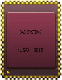 |
POWER | 32 bits | 1 | 0.5 μm | 1.1 M | 8 KB unified | n/a | n/a | 20–33 MHz | Rad hard | 1997 | |
| POWER3 |  |
POWER2 PowerPC 1.1 |
64 bits | 1 | 0.35 μm | 15 M | 270 mm2 | 32 KB I 64 KB D |
1–16 MB external |
n/a | 200–222 MHz | 1088 pin CLGA | 1998 |
| POWER3-II |  |
POWER2 PowerPC 1.1 |
64 bits | 1 | 0.25 μm Cu | 23 M | 170 mm2 | 32 KB I 64 KB D |
1–16 MB external |
n/a | 333–450 MHz | 1088 pin CLGA | 1999 |
| POWER4 |  |
PowerPC 2.00 PowerPC-AS |
64 bits | 2 | 180 nm | 174 M | 412 mm2 | 64 KB I 32 KB D per core |
1.41 MB per core |
32 MB external |
1–1.3 GHz | 1024 pin CLGA ceramic MCM |
2001 |
| POWER4+ |  |
PowerPC 2.01 PowerPC-AS |
64 bits | 2 | 130 nm | 184 M | 267 mm2 | 64 KB I 32 KB D per core |
1.41 MB per chip |
32 MB external |
1.2–1.9 GHz | 1024 pin CLGA ceramic MCM |
2002 |
| POWER5 |  |
PowerPC 2.02 Power ISA 2.03 |
64 bits | 2 | 130 nm | 276 M | 389 mm2 | 32 KB I 32 KB D per core |
1.875 MB per chip |
32 MB external |
1.5–1.9 GHz | ceramic DCM ceramic MCM |
2004 |
| POWER5+ |  |
PowerPC 2.02 Power ISA 2.03 |
64 bits | 2 | 90 nm | 276 M | 243 mm2 | 32 KB I 32 KB D per core |
1.875 MB per chip |
32 MB external |
1.5–2.3 GHz | ceramic DCM ceramic QCM ceramic MCM |
2005 |
| POWER6 |  |
Power ISA 2.03 | 64 bits | 2 | 65 nm | 790 M | 341 mm2 | 64 KB I 64 KB D per core |
4 MB per core |
32 MB external |
3.6–5 GHz | CLGA OLGA |
2007 |
| POWER6+ |  |
Power ISA 2.03 | 64 bits | 2 | 65 nm | 790 M | 341 mm2 | 64 KB I 64 KB D per core |
4 MB per core |
32 MB external |
3.6–5 GHz | CLGA OLGA |
2009 |
| POWER7 |  |
Power ISA 2.06 | 64 bits | 8 | 45 nm | 1.2 B | 567 mm2 | 32 KB I 32 KB D per core |
256 KB per core |
32 MB per chip |
2.4–4.25 GHz | CLGA OLGA organic QCM |
2010 |
| POWER7+ |  |
Power ISA 2.06 | 64 bits | 8 | 32 nm | 2.1 B | 567 mm2 | 32 KB I 32 KB D per core |
256 KB per core |
80 MB per chip |
2.4–4.4 GHz | OLGA organic DCM |
2012 |
| POWER8 |  |
Power ISA 2.07 | 64 bits | 6 12 |
22 nm | ?? 4.2 B |
362 mm2 649 mm2 |
32 KB I 64 KB D per core |
512 KB per core |
48 MB 96 MB per chip |
2.75-4.2 GHz | OLGA DCM OLGA SCM |
2014 |
| POWER8 with NVLink |
Power ISA 2.07 | 64 bits | 12 | 22 nm | 4.2 B | 659 mm2 | 32 KB I 64 KB D per core |
512 KB per core |
48 MB 96 MB per chip |
3.26 GHz | OLGA SCM | 2016 | |
| POWER9 SU | Power ISA 3.0 | 64 bits | 12 24 |
14 nm | 8 B | 32 KB I 64 KB D per core |
512 KB per core |
120 MB per chip |
~4 GHz | 2017 | |||
| Name | Image | ISA | Bits | Cores | Fab | Transistors | Die size | L1 | L2 | L3 | Clock | Package | Introduced |
See also
References
- ↑ The Four Hundred-Some Insight Into Those Future Power7+ Processors
- ↑ IBM Power Systems 2013.
- ↑ Linux-Kernel Archive: [git pull] Please pull powerpc.git next branch
- ↑ You won't find this in your phone: A 4 GHz 12-core Power8 for badass boxes
- ↑ Add full Power ISA 3.0 / POWER9 binutils support
- ↑ NVIDIA Volta GPUs and IBM Power9 CPUs To Deliver Up To 300 PetaFlops of Performance in 2017 With Summit and Sierra Supercomputers
- ↑ NVIDIA Volta, IBM POWER9 Land Contracts For New US Government Supercomputers
- ↑ ORNL Summit home page
- ↑ Lawrence Livermore signs contract with IBM
- ↑ Power9: Google gives Intel a chip-flip migraine, IBM tries to lures big biz