Threshold voltage
The threshold voltage, commonly abbreviated as Vth or VGS (th), of a field-effect transistor (FET) is the minimum gate-to-source voltage differential that is needed to create a conducting path between the source and drain terminals.
When referring to a junction field-effect transistor (JFET), the threshold voltage is often called "pinch-off voltage" instead. This is somewhat confusing since "pinch off" applied to insulated-gate field-effect transistor (IGFET) refers to the channel pinching that leads to current saturation behaviour under high source–drain bias, even though the current is never off. Unlike "pinch off", the term "threshold voltage" is unambiguous and refers to the same concept in any field-effect transistor.
Basic principles
In n-channel enhancement-mode devices, a conductive channel does not exist naturally within the transistor, and a positive gate-to-source voltage is necessary to create one. The positive voltage attracts free-floating electrons within the body towards the gate, forming a conductive channel. But first, enough electrons must be attracted near the gate to counter the dopant ions added to the body of the FET; this forms a region with no mobile carriers called a depletion region, and the voltage at which this occurs is the threshold voltage of the FET. Further gate-to-source voltage increase will attract even more electrons towards the gate which are able to create a conductive channel from source to drain; this process is called inversion.
In contrast, n-channel depletion-mode devices have a conductive channel naturally existing within the transistor. Accordingly, the term 'threshold voltage' does not readily apply to turn such devices 'on', but is used instead to denote the voltage level at which the channel is wide enough to allow electrons to flow easily. This ease-of-flow threshold also applies to p-channel depletion-mode devices, in which a positive voltage from gate to body/source creates a depletion layer by forcing the positively charged holes away from the gate-insulator/semiconductor interface, leaving exposed a carrier-free region of immobile, negatively charged acceptor ions.
In wide planar transistors the threshold voltage is essentially independent of the drain–source voltage and is therefore a well defined characteristic, however it is less clear in modern nanometer-sized MOSFETs due to drain-induced barrier lowering.


In the figures, the source (left side) and drain (right side) are labeled n+ to indicate heavily doped (blue) n-regions. The depletion layer dopant is labeled NA− to indicate that the ions in the (pink) depletion layer are negatively charged and there are very few holes. In the (red) bulk the number of holes p = NA making the bulk charge neutral.
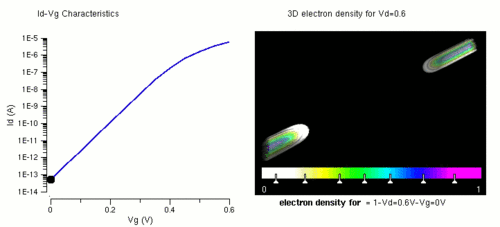
If the gate voltage is below the threshold voltage (top figure), the transistor is turned off and ideally there is no current from the drain to the source of the transistor. In fact, there is a current even for gate biases below the threshold (subthreshold leakage) current, although it is small and varies exponentially with gate bias.
If the gate voltage is above the threshold voltage (lower figure), the transistor is turned on, due to there being many electrons in the channel at the oxide-silicon interface, creating a low-resistance channel where charge can flow from drain to source. For voltages significantly above the threshold, this situation is called strong inversion. The channel is tapered when VD > 0 because the voltage drop due to the current in the resistive channel reduces the oxide field supporting the channel as the drain is approached.
Body effect
The body effect is the change in the threshold voltage by an amount approximately equal to the change in , the source-bulk voltage. Because the body influences the threshold voltage (when it is not tied to the source), it can be thought of as a second gate, and is sometimes referred to as the "back gate"; the body effect is sometimes called the "back-gate effect".[1]

For an enhancement mode, nMOS MOSFET body effect upon threshold voltage is computed according to the Shichman–Hodges model[2] (accurate for very old technology) using the following equation.

where is the threshold voltage when substrate bias is present, is the source-to-body substrate bias, is the surface potential, and is threshold voltage for zero substrate bias, is the body effect parameter, is oxide thickness, is oxide permittivity, is the permittivity of silicon, is a doping concentration, is the charge of an electron.


Dependence on oxide thickness
In a given technology node, such as the 90-nm CMOS process, the threshold voltage depends on the choice of oxide and on oxide thickness. Using the body formulas above, is directly proportional to , and , which is the parameter for oxide thickness.


Thus, the thinner the oxide thickness, the lower the threshold voltage. Although this may seem to be an improvement, it is not without cost; because the thinner the oxide thickness, the higher the subthreshold leakage current through the device will be. Consequently, the design specification for 90-nm gate-oxide thickness was set at 1 nm to control the leakage current.[3] This kind of tunneling, called Fowler-Nordheim Tunneling.[4]

where and are constants and is the electric field across the gate oxide.


Before scaling the design features down to 90 nm, a dual-oxide approach for creating the oxide thickness was a common solution to this issue. With a 90 nm process technology, a triple-oxide approach has been adopted in some cases.[5] One standard thin oxide is used for most transistors, another for I/O driver cells, and a third for memory-and-pass transistor cells. These differences are based purely on the characteristics of oxide thickness on threshold voltage of CMOS technologies.
Dependence on temperature
As with the case of oxide thickness affecting threshold voltage, temperature has an effect on the threshold voltage of a CMOS device. Expanding on part of the equation in the body effect section

where is half the contact potential, is Boltzmann's constant, is Temperature, is the charge of an electron, is a doping parameter and is the intrinsic doping parameter for the substrate.


We see that the surface potential has a direct relationship with the temperature. Looking above, that the threshold voltage does not have a direct relationship but is not independent of the effects. On average this variation is between −4 mV/K and −2 mV/K depending on doping level.[6] For a change of 30 °C this results in significant variation from the 500 mV design parameter commonly used for the 90 nm technology node.
Dependence on random dopant fluctuation
Random dopant fluctuation(RDF) is a form of process variation resulting from variation in the implanted impurity concentration. In MOSFET transistors, RDF in the channel region can alter the transistor's properties, especially threshold voltage. In newer process technologies RDF has a larger effect because the total number of dopants is fewer.[7]
Research works are being carried out in order to suppress the dopant fluctuation which leads to the variation of threshold voltage between devices undergoing same manufacturing process.[8]
See also
References
- ↑ Marco Delaurenti, PhD dissertation, Design and optimization techniques of high-speed VLSI circuits (1999))
- ↑ NanoDotTek Report NDT14-08-2007, 12 August 2007
- ↑ Sugii, Watanabe and Sugatani. Transistor Design for 90-nm Generation and Beyond. (2002)
- ↑ S. M. Sze, Physics of Semiconductor Devices, Second Edition, New York: Wiley and Sons, 1981, pp. 496–504.
- ↑ Anil Telikepalli, Xilinx Inc, Power considerations in designing with 90 nm FPGAs (2005))
- ↑ Weste and Eshraghian, Principles of CMOS VLSI Design : a systems perspective, Second Edition, (1993) pp.48 ISBN 0-201-53376-6
- ↑ Asenov, A. Huang,Random dopant induced threshold voltage lowering and fluctuations in sub-0.1 μm MOSFET's: A 3-D “atomistic” simulation study, Electron Devices, IEEE Transactions, 45 , Issue: 12
- ↑ Asenov, A. Huang,Suppression of random dopant-induced threshold voltage fluctuations in sub-0.1-μm MOSFET's with epitaxial and δ-doped channels, Electron Devices, IEEE Transactions, 46, Issue: 8
External links
- Online lecture on: Threshold Voltage and MOSFET Capacitances by Dr. Lundstrom