Extreme ultraviolet lithography
.svg.png)
Extreme ultraviolet lithography (also known as EUV or EUVL) is a next-generation lithography technology using an extreme ultraviolet (EUV) wavelength, currently expected to be 13.5 nm. EUV is currently being developed for possible future high volume use in 2020.[1][2][3][4] The primary EUV tool maker, ASML, projects EUV at 5 nm node to require a higher numerical aperture than currently available and multiple patterning to a greater degree than immersion lithography at 20 nm node.[5] Immersion lithography is still roughly 3 times faster than EUV, due to source power limitations. In October 2016, ASML has said its EUV tools can make almost 1500 wafers per day but has not met 90% uptime, while conventional tools do 5000 wafers per day with 95% uptime.[6] Hence, multiple patterning with immersion lithography has already been used where EUV had previously been expected to be used.
While source power is the chief concern due to its impact on productivity, significant changes in EUV mask infrastructure, including blanks, pellicles and inspection, are also under study. Particle contamination would be prohibitive if pellicles were not stable above 200 W, i.e., the targeted power for manufacturing.[7] Without pellicles, particle adders would reduce yield, which has not been an issue for conventional optical lithography with 193 nm light and pellicles. The current lack of any suitable pellicle material, aggravated by the use of hydrogen plasma cleaning in the EUV scanner,[8][9] is preventing the adoption of EUV lithography for volume production.[10]
Secondary electron effects (covered below) degrade resolution at the targeted insertion nodes.[11]
Some issues not specific to EUV, such as resist collapse[12] and stochastic effects (including photon shot noise),[13] also currently bar EUV from exceeding the resolution limits of immersion lithography in high volume manufacturing.[14]
Double patterning is expected for EUV for random logic patterns at the 7 nm node (32 nm pitch), due to the need for dipole illumination.[15] The 5 nm node (22 nm pitch)[16] would likewise be expected to use multiple patterning already being developed for immersion lithography.
Light source
Neutral atoms or condensed matter cannot emit EUV radiation. Ionization must precede EUV emission in matter. Electrons must be bound to multicharged positive ions; for example, to remove an electron from a +3 charged carbon ion (three electrons already removed) requires about 65 eV.[17] Such electrons are more tightly bound than typical valence electrons. The thermal production of multicharged positive ions is only possible in a hot dense plasma, which itself strongly absorbs EUV.[18] As of 2016, the established EUV light source is a laser-pulsed Sn plasma,[19] where the source of 13.5 nm light is an unstable population of Sn+9, Sn+10, Sn+11(average), Sn+12, and Sn+13 ions;[20] these ions also absorb the light they emit, and are easily neutralized by electrons in the plasma to lower charge states which produce light mainly at other, unusable wavelengths, which results in a much reduced efficiency of light generation for lithography at higher plasma power density.
Xe or Sn plasma sources are either discharge-produced or laser-produced. Discharge-produced plasma is made by discharging a lightning bolt's worth of electric current through a tin vapor. Laser-produced plasma is made by microscopic droplets of molten tin heated by powerful laser. Laser-produced plasma sources (e.g., ASML's NXE:3300B scanner) outperform discharge-produced plasma sources. Power output exceeding 250 W is a requirement for sufficient throughput.
While state-of-the-art 193 nm ArF excimer lasers offer intensities of 200 W/cm2,[21] lasers for producing EUV-generating plasmas need to be much more intense, on the order of 1011 W/cm2.[22] This indicates the enormous energy burden imposed by switching from 193 nm light (power output approaching 100 W)[23] to EUV light (10 kW).[24] An EUV source driven by a 200 kW CO2 laser with ~10% wall plug efficiency[25] consumes an electrical power of ~2 MW, while a 100 W ArF immersion laser with ~1% wall plug efficiency[26] consumes an electrical power of ~10 kW. A state-of-the-art ArF immersion lithography 120 W light source requires no more than 40 kW[27] while EUV sources are targeted to exceed 40 kW.[28]
A further characteristic of the plasma-based EUV sources under development is that they are not even partially coherent,[29] unlike the KrF and ArF excimer lasers used for current optical lithography. Further power reduction (energy loss) is expected in converting incoherent sources (emitting in all possible directions at many independent wavelengths) to partially coherent (emitting in a limited range of directions within a narrow wavelength band) sources by filtering. Coherent light poses a risk of monochromatic reflection interference and mismatch of multilayer reflectance bandwidth.[30]
As of 2008, development tools had a throughput of 4 wafers per hour with a 120 W source.[31] For a 100 WPH requirement, therefore, a 3 kW source would be needed, which was not expected to be available in the foreseeable future. However, EUV photon count is determined by the number of electrons generated per photon that are collected by a photodiode. This is essentially the highly variable secondary yield of the initial photoelectron, yielding highly variable dose measurement. Data by Gullikson et al.[32] indicated ~10% natural variation of the photocurrent responsivity. More recent data for silicon photodiodes agree with this assessment.[33] Calibration of the EUV dosimeter remained a nontrivial unsolved issue.[34] The secondary electron number variability is the well-known root cause of noise in avalanche photodiodes.[35]
The highly relativistic vacuum tube free-electron lasers and synchrotron radiation sources can give better light quality than material sources, though high intensity may require development work. Existing dedicated industrial synchrotron light facilities with applications including semiconductor device fabrication. Free electron lasers offer light that is monochromatic and coherent, as well as narrow in space and angle spread. Both also offer a continuous range of available wavelengths, allowing seamless progress into the X-ray band.[36]
At SPIE 2014, TSMC reported that the 200 kW CO2 laser for their NXE:3100 EUV tool light source had a misalignment problem.[37] The laser was supposed to focus on a tin droplet that absorbs the power to generate EUV light. Missing the droplet directed the power elsewhere, leading to component damage and downtime.
As of September 2015, ASML demonstrated EUV tools with light source power of 130W and over 70% uptime at multiple customer sites, but only for limited one-week periods, over four weeks in one case. [38]
Optics


EUVL is a significant departure from the deep ultraviolet lithography standard. All matter absorbs EUV radiation. Hence, EUV lithography requires a vacuum. All optical elements, including the photomask, must use defect-free Mo/Si multilayers that act to reflect light by means of interlayer interference; any one of these mirrors absorb around 30% of the incident light. This limitation can be avoided in maskless interference lithography systems. However, the latter tools are restricted to periodic patterns only.
Current EUVL systems contain at least two condenser multilayer mirrors, six projection multilayer mirrors and a multilayer object (mask). Since the optics already absorbs 96% of the EUV light, the ideal EUV source will need to be much brighter than its predecessors. EUV source development has focused on plasmas generated by laser or discharge pulses. The mirror responsible for collecting the light is directly exposed to the plasma and is therefore vulnerable to damage from high-energy ions[39][40] and other debris.[41] This damage has precluded EUV light sources from success.
Another aspect of EUVL tools is the off-axis illumination (at an angle of 6 degrees)[42] on a multilayer mask. The resulting asymmetry (leading to non-telecentricity) in the diffraction pattern causes shadowing effects that degrade pattern fidelity.[43]
EUVL's shorter wavelength also increases flare, resulting in less than perfect image quality and increased line width roughness.[44]
Heating per feature volume (e.g., 20 nm cube) is higher per EUV photon compared DUV photons, due to higher absorption in resist. In addition, EUV lithography results in more heating due to the vacuum environment, in contrast to the water cooled environment of immersion lithography. Most of the EUV source energy is absorbed by the multilayer mirrors with the rest being used to actually expose the resist.[45]
Heating is also a particularly serious issue for multilayer mirrors. As EUV is absorbed close to the surface, the heating density is higher. As a result, water cooling is expected to be used, producing vibration that is a concern.[46]
Heating of the EUV mask pellicle (film temperature up to 750 K for 80 W incident power) is a significant concern, due to the resulting deformation and transmission decrease.[47]
A recent study found that multilayer optics contamination was highly affected by the resonant structure of the EUV mirror, influencing photoelectron generation and secondary electron yield.[48]
Since EUV is highly absorbed by all materials, even EUV optical components inside the lithography tool are susceptible to damage, mainly manifest as observable ablation.[49] Such damage is specific to EUV lithography, as conventional optical lithography systems use mainly transmissive components and do not put any component in the way of electrons, although these electrons end up depositing energy in the exposed sample substrate.
In 2012, researchers reported that a Ru-capped Mo/Si multilayer could be damaged by a single pulse (16° incidence at 13.5 nm) as low as 30 mJ/cm2, and the damage threshold can be lowered ~60% with ten pulses.[50] This was attributed to the cumulative probability of defect occurrence with multiple pulses.
Another collaboration study in 2010,[51] using Mo/Si multilayers with 42–44% reflectivity at ~28° incidence, started showing damage for single pulse at a level of ~45 mJ/cm2.
Overlay issues

Because EUV operates in a vacuum and requires reflective optics, EUV lithography tools have special overlay concerns, recently studied by IMEC, along with ASML.[52] Electrostatic chucks must be used instead of conventional vacuum chucks. Therefore, the wafer clamping variability on the electrostatic chuck needs to be dealt with. A backside coating of 200 nm silicon nitride (which must be removed later to allow backside cooling[53] and heatsinking[54][55]) was found to be helpful. Other than this additional step, which also requires first protecting the device layers already patterned,[56][57] zone alignment (using all alignment marks across the wafer, not a standard subset) also provided some improvement. The vacuum environment required by EUV also leads to heating of the wafer without much dissipation. A sacrificial first wafer was found to be necessary to stabilize the chuck temperature. Moreover, the local overlay corrections due to exposure heating requires the use of a second wafer. Thus, an extra wafer per lot is required for overlay stabilization in EUV lithography. The use of reflection causes wafer exposure position to be extremely sensitive to the reticle flatness and the reticle clamp. Reticle clamp cleanliness is therefore required to be maintained.
The off-axis illumination of the reticle is also the cause of non-telecentricity in wafer defocus, which consumes most of the overlay budget of the NXE:3300 EUV scanner[58] even for design rules as loose as 100 nm pitch.[59]
More significantly, mask defocus has been found to result in even larger overlay errors.[60][61] Hence, features at different locations will shift differently due to different deviations from flatness.
Possibly the most significant pattern shift error comes from even small (mrad-scale) deviations in mask flatness in the local slope, coupled with wafer defocus.[62]
Photoresist exposure
When an EUV photon is absorbed, photoelectrons and secondary electrons are generated by ionization, much like what happens when X-rays or electron beams are absorbed by matter.[63] It has been estimated that about 4 secondary electrons on average are generated for every EUV photon, although the generation volume is not definite.[64] These secondary electrons have energies of a few to tens of eV and travel tens of nanometers inside photoresist (see below) before initiating the desired chemical reaction. This is very similar to the photoelectron migration for the latent image formation in silver halide photographic films. A contributing factor for this rather large distance is the fact that polymers have significant amounts of free volume.[65] In a recent actual EUV print test,[66] it was found 30 nm spaces could not be resolved, even though the optical resolution and the photoresist composition were not the limiting factor. In particular, for photoresists utilizing chemical amplification for higher throughput:[67][68]
e− + acid generator -> anion -> dissociated anion products
This reaction, also known as "electron attachment" or "dissociative electron attachment" is most likely to occur after the electron has essentially slowed to a halt, since it is easiest to capture at that point. The cross-section for electron attachment is inversely proportional to electron energy at high energies, but approaches a maximum limiting value at zero energy.[69] On the other hand, it is already known that the mean free path at the lowest energies (few to several eV or less, where dissociative attachment is significant) is well over 10 nm,[70][71] thus limiting the ability to consistently achieve resolution at this scale. In addition, electrons with energies < 20 eV are capable of desorbing hydrogen and fluorine anions from the resist,[72] leading to potential damage to the EUV optical system.[73]
EUV photoresist images often require resist thicknesses roughly equal to the pitch.[74] This is not only due to EUV absorption causing less light to reach the bottom of the resist but also to forward scattering from the secondary electrons (similar to low-energy electron beam lithography). Conversely, thinner resist transmits a larger fraction of incident light allowing damage to underlying films, yet requires more dosage to achieve the same level of absorption.
Since the photon absorption depth exceeds the electron escape depth, as the released electrons eventually slow down, they dissipate their energy ultimately as heat.
An EUV dose of 1 mJ/cm2 generates an equivalent photoelectron dose of 10.9 μC/cm2. Current demonstration doses exceed 10 mJ/cm2, or equivalently, 109 μC/cm2 photoelectron dose.
The use of higher doses and/or reduced resist thicknesses to produce smaller features only results in increased irradiation of the layer underneath the photoresist. This adds another significant source of photoelectrons and secondary electrons which effectively reduce the image contrast. In addition, there is increased possibility of ionizing radiation damage to the layers below.
The extent of secondary electron and photoelectrons in blurring the resolution is dependent on factors such as dose, surface contamination, temperature, etc.
It should be noted that EUV resists are also exposable by wavelengths longer than EUV, particular VUV and DUV wavelengths in the 150–250 nm range.[75]
Point spread function of resist
Kozawa et al. determined the point spread function of EUV chemically amplified resists using a basic acid generation calculation and simulation fit. The range of acid generation extended ~20 nm from the absorption point, entailing a ~40 nm resolution limit.[76]
Given that photoresists easily diffuse acid molecules, it would be no surprise that the smaller and lighter electrons produced by EUV or other ionizing radiation would diffuse faster and further, rendering the expected optical resolution meaningless.
The resist blur based on print results at the end of 2008 is in the range of 10–16 nm.[77] Half-pitch resolution is still a struggle below 30 nm, and line edge roughness is still a major issue.
A study in 2011 focusing on 22 nm and 24 nm half-pitch indicated a temperature-dependent blur for the post-exposure bake process, ranging from ~5 nm at 80 °C to ~10 nm at ~110 °C. The secondary electron blur was reported to be not observed in this range.[78] The aerial images were corrected for the estimated flare (which would include any long-range secondary electron blur).
Efficient photoresist heating
Ritucci et al., reported on the improved thermal ablation efficiency for EUV wavelengths compared to DUV wavelengths.[79] Since EUV exceeds the bandgap of all materials, it is more easily absorbed than longer wavelengths, and the same dose of incident energy results in more heating; even ~100 mJ/cm2 would be hot enough to result in ablation. The resolution of chemically amplified photoresists is determined by thermally driven acid diffusion (spreading). It is worth noting that even at the ablation dose of 100 mJ/cm2, the shot noise for a 1 nm pixel is still significant (3σ/avg = 36%), which could severely impact a critical dimension (CD) for which the pixel is at least 5%, i.e., 20 nm or less.
Resist outgassing

Due to the high efficiency of absorption of EUV by photoresists, heating and outgassing become primary concerns. Organic photoresists outgas hydrocarbons[80] while metal oxide photoresists outgas water and oxygen[81] The carbon contamination is known to affect multilayer reflectivity[82] while the oxygen is particularly harmful for the ruthenium capping layers on the EUV multilayer optics.[83]
Resist polymer aggregates
Resists as polymers are well-known to have aggregates with sizes up to 80 nm.[84] Even the high-resolution resist HSQ has aggregate size reduced down to only 15–20 nm.[85] While the roughness of lines larger than the aggregate size are mildly affected by the aggregate size, below the aggregate size obviously the linewidth can be severely affected.
Resist line roughness
A model for resist line roughness caused by defects proposed in 1994 predicted that if minimum EUV dose levels for a given linewidth were not met, the resulting roughness from sidewall or base defects would be prohibitive.[86] For 20 nm linewidth and below, the minimum dose easily exceeds 100 mJ/cm2 for resists that are not chemically amplified.
Defects
EUVL faces specific defect issues analogous to those being encountered by immersion lithography. Whereas the immersion-specific defects are due to unoptimized contact between the water and the photoresist, EUV-related defects are attributed to the inherently ionizing energy of EUV radiation. The first issue is positive charging, due to ejection of photoelectrons[87] freed from the top resist surface by the EUV radiation. This could lead to electrostatic discharge or particle contamination as well as the device damage mentioned above. A second issue is contamination deposition on the resist from ambient or outgassed hydrocarbons, which results from EUV- or electron-driven reactions.[88] A third issue is etching of the resist by oxygen,[89] argon or other ambient gases, which have been dissociated by the EUV radiation or the electrons generated by EUV. Ambient gases in the lithography chamber may be used for purging and contamination reduction. These gases are ionized by EUV radiation, leading to plasma generation in the vicinity of exposed surfaces, resulting in damage to the multilayer optics and inadvertent exposure of the sample.[90]


Of course mask defects are also a known source of defects for EUVL. Reducing defects on extreme ultraviolet (EUV) masks is currently one of the most critical issues to be addressed for commercialization of EUV lithography.[91] The defect core, namely the pit or particle, can originate either on the substrate, during multilayer deposition or on top of the multilayer stack. Mesas or protrusions form on the sputtering targets used for multilayer deposition, which may fall off as particles during the multilayer deposition.[92] The printability of the final defect will depend on the phase change and the amplitude change of light at a given position. The net phase change and/or amplitude change adds to the intrinsic effect of the core defect and its influence on the growth of the multilayer stack during deposition. The buried defects are particularly insidious.[93]
The phase shift caused by an undetected substrate flatness variation is sufficient to produce a printable defect. The principle behind this is a quarter-wavelength deviation from the flat surface produces a half-wavelength optical path difference after reflection. The light that is reflected from the flat surface is 180 degrees out of phase with the light reflected from the quarter-wavelength deviation.[94] In fact, defects of atomic scale height (0.3–0.5 nm) with 100 nm FWHM can still be printable by exhibiting 10% CD impact.[95] IBM and Toppan reported at Photomask Japan 2015 that smaller defects, e.g., 50 nm size, can have 10% CD impact even with 0.6 nm height, yet remain undetectable.[96] Like a lens, any defect which effectively produces a phase shift scatters light outside the defect region. The amount of light that is scattered can be calculated. Furthermore, the edge of a phase defect will further reduce reflectivity by more than 10% if its deviation from flatness exceeds 3 degrees, due to the deviation from the target angle of incidence of 84 degrees with respect to the surface. Even if the defect height is shallow, the edge still deforms the overlying multilayer, producing an extended region where the multilayer is sloped. The more abrupt the deformation, the narrower the defect edge extension, the greater the loss in reflectivity.
EUV mask defect repair is also more complicated due to the across-slit illumination variation mentioned above. Due to the varying shadowing sensitivity across the slit, the repair deposition height must be controlled very carefully, being different at different positions across the EUV mask illumination slit.[97]
Pellicles
Pellicles are normally expected to protect the mask from falling particles during exposure. However, for EUV, the feasibility of pellicle use is severely challenged, due to the required thinness of the shielding films to prevent excessive EUV absorption. For example, ASML developed a 70 nm thick polysilicon pellicle membrane, which allows EUV transmission of 82%; however, less than half of the membranes survived expected EUV power levels.[98] SiNx pellicle membranes also failed at 82 W equivalent EUV source power levels.[99] Alternative materials need to allow sufficient transmission as well as maintain mechanical and thermal stability. However, graphene or other carbon nanomaterials (nanosheets, nanotubes) are damaged by EUV[100] and also too easily etched in the hydrogen cleaning plasma expected to be deployed in EUV scanners.[101] Hydrogen plasmas can also etch silicon as well.[102][103]
Line edge roughness from mask surface roughness
The much shorter wavelength of EUV (13.5 nm) makes it more sensitive to phase fluctuations from surface roughness. Even a practical, atomic-level flatness of 0.23 nm leads to a prohibitive 2.3 nm line edge roughness (LER) for 22 nm lines and spaces, for the largest degree of coherence (expected with the use of off-axis illumination) studied.[104]
Projection optics scaling limits
The reduced wavelength of EUV (13.5 nm) is one factor in resolution. The other is the numerical aperture (NA) of the tool. Due to the off-axis reflective nature of the optical system, increasing NA for higher resolution is not so straightforward.
Angle of incidence
The reflective nature of the optics requires an off-axis angle of incidence onto the mask containing the pattern. For the smallest allowed pitches, the angle of incidence is extremely restricted to the Bragg's Law condition so that the smallest angle with the surface normal is given by[105] sin(minimum angle)=sin(incident angle)−0.5×wavelength/(4×pitch), with 4 being the demagnification factor (ratio of mask line pitch to target line pitch). For a wavelength of 13.5 nm and an axis-defined incident angle of 6°, a pitch of 16 nm leads to a minimum angle below 0, which is forbidden. Practically, the minimum line pitch should therefore be 19–20 nm to allow a minimum angle of 1°, 28 nm to allow the minimum angle to be reduced 2.5°. To reduce the minimum pitch, either the wavelength must be reduced or the axis-defined angle of incidence increased. When increasing the axis-defined angle of incidence, the range of all possible angles of incidence (inversely proportional to the minimum pitch, from the above equation) increases as well, requiring a larger angular bandwidth for all the multilayers making up the EUV optical components, not just the mask. This will require a significant change to the existing EUV infrastructure.
.png)
Diffraction and multilayer angle bandwidth
Resolution requirements below 20 nm require higher numerical aperture (N.A.) EUV optical systems supported by multilayer optics. However, the larger aperture necessarily entails larger angles of incidence as well as a larger range of incident angles. The multilayer currently used in EUV masks and optical systems tends to attenuate light at larger angles which is required to image tighter pitches. In particular, apodization (non-uniformity of intensity across the light entrance pupil), due to different reflectivity at different angles, becomes more severe for higher numerical apertures.[106]

For 2D patterns like dense contact holes, contrast already decreases from 80% to <75% going from 19 nm to 18 nm half-pitch, 14 nm half-pitch is already in need of multilayer tuning, and in fact, without the use of increased demagnification (above 4X) to help reduce the angles, no imaging beyond ~13 nm half-pitch is possible.[108] Such demagnification would result in large photomask substrate sizes or else multiple small fields (on different masks).
In fact, for EUV mask pitches of 8 wavelengths or less (demagnified 4x to 2 wavelengths (13–14 nm half-pitch) or less on the wafer), diffraction into the multilayer at larger angles is another source of significant image degradation, which requires intensive computation to evaluate.[109] For larger angles, the multilayer reflectance decreases significantly.[110] Rigorous EM simulations for the EUV binary mask at different magnifications have already indicated that for the standard 4X magnification, the diffraction order efficiencies starts varying significantly with new asymmetry (non-telecentricity) below 20 nm half-pitch.[111]
Telecentricity considerations alone indicate substantial difficulty using EUV below 28 nm half pitch, due to worsening telecentricity error.[112]
Etched multilayer masks[113] have been proposed to alleviate the above issues, but actually this requires the patterning of high aspect-ratio (>3.5) features on the EUV mask itself, which could lead to pattern collapse limiting the resolution to >80 nm on the mask (i.e., >20 nm on the wafer with 4x magnification).
Mask absorber thickness variation and border effect
A study published in 2011 by ASML, Brion and Zeiss found that EUV mask absorber thickness has significant effect on exposure latitude and mask error enhancement.[114] This was observed at 27-32 nm half-pitch. Furthermore, the effects were noticeably different for different conventional illumination settings. For example, for 32 nm line-and-space patterns, the optimum dose-to-size differed by more than 30%, while best bias differed by more than 4 nm, between 55.4 nm and 58 nm thickness (+/- 2.3% thickness variation). The mask absorber thickness could be optimized for size and exposure latitude for different conventional mask patterns. There remains a tradeoff of exposure latitude vs. throughput. The absorber still allows some fraction of light to pass in one direction, and the top surface itself reflects some light. The optimum absorber thickness is a linear function of the half-pitch, as well as the range of incident angles.[115] Even at the optimum absorber thickness, there is sufficient reflectivity (EUV or DUV) to present a field-to-field flare effect from the mask border. The shadowing effect is more obvious with thicker absorber.[116] The absorber thickness needs to be tightly controlled across the mask and from mask-to-mask to prevent proximity matching errors. Furthermore, the absorber thickness needs to be considered for OPC determination. With a typical CD sensitity of around 1 nm/cm2, for 27-32 nm lines, the issue is severe enough that there is a proposal to completely etch away the absorber and multilayer at the mask image field border, which entails a second layer or level of patterning in the mask fabrication, as in the case of a phase-shift mask.[117]
Source-mask optimization
Due to the effects of non-telecentricity, standard illumination pupil shapes, such as disc or annular, are not sufficient to be used for feature sizes of ~20 nm or below (10 nm node and beyond).[59] Instead certain parts of the pupil (often over 50%) must be asymmetrically excluded. The parts to be excluded depend on the pattern. There may be 200–400 illuminating points, each contributing its weight of the dose to balance the overall image through focus. Thus the shot noise effect (to be discussed later) critically affects the image position through focus, in a large population of features.
Throughput vs. resolution
The resolution of EUV lithography for future advanced faces challenges in maintaining throughput, i.e., how many wafers are processed by an EUV tool per day. These challenges arise from smaller fields, additional mirrors, and shot noise. In order to maintain throughput, the power at intermediate focus (IF) must be continually increased.
Reduced fields

Preparation of an anamorphic lens with an NA between 0.5 and 0.6 is underway as of 2016. The demagnification will be 8X in one dimension and 4X in the other, and the angle of reflection will increase.[118]
Higher demagnification will increase the mask size or reduce the size of the printed field. Reduced field size would divide full-size chip patterns (normally taking up 26 mm × 33 mm) among two or more conventional 6-inch EUV masks. Large (approaching or exceeding 500 mm2) chips, typically used for GPUs[119] or servers,[120] would have to be stitched together from two or more sub-patterns from different masks.[121] Without field stitching, die size would be limited. With field stitching, features that cross field boundaries would have alignment errors, and the extra time required to change masks would reduce the throughput of the EUV system.[122]
Additional mirrors
As each mirror results in reflecting ~70% of the light, adding two mirrors to a 6-mirror system would result in a 50% reduction of throughput.[123]
Shot noise: the statistical resolution limit

The difference between 21 nm diameter and 19 nm diameter is a little over 60 square nanometers. A dose of 50 mJ/cm2 means only about 2000 EUV photons in such a small edge area. With the natural Poisson distribution due to the random arrival times of the photons, there is an expected natural dose variation of at least several percent 3 sigma, making the exposure process susceptible to stochastic variations. The dose variation leads to a variation of the feature edge position, effectively becoming a blur component. Unlike the hard resolution limit imposed by diffraction, shot noise imposes a softer limit, with the main guideline being the ITRS line width roughness (LWR) spec of 8% (3s) of linewidth.[124] Increasing the dose will reduce the shot noise, but will also increase the flare dose and generate more free electrons. The free electrons will spread out before slowing to a stop. Since the free electron density is even lower than the initial photon density, the shot noise is always effectively larger than expected from just considering the EUV dose.
For 10nm-node SRAM local interconnect (62 nm pitch), there was noticeable printability dependence on dose, indicating the stochastic impact of shot noise.[13]
The shot noise has strong bearing on the EUV source power issue mentioned above. For 10 mJ/cm2, the power at intermediate focus should be 180 W; currently it is about 20 W at high duty cycle.[125] However, significant shot noise may force minimum doses to be at least 42 mJ/cm2 for 20 nm feature size (e.g., 20 nm cuts in 20 nm half-pitch lines) and 169 mJ/cm2 for 10 nm feature size (e.g., 10 nm contacts on 14 nm half-pitch lines), therefore indicating the EUV source power to be a moving target becoming ever more difficult to reach.[126] These minimum dose values already exceed the multilayer pulse damage thresholds indicated above. Actually, the most widely acknowledged concern of such high doses is the increased resist ougassing (30 mJ/cm2 being prohibitive).[127] Crosslinking also becomes apparent as terminal C=C double bonds are reduced as dose is more than doubled.[128] As discussed below, due to high absorption, heating is more significant.
For chemically amplified resists, higher dose exposure also increases line edge roughness due to acid generator decomposition.[129]
The most sensitive indicator of shot noise are features which are very sensitive to dose. A prime example is the tip-to-tip space between line ends.[15] The exposure latitude is inherently worse. For 10 nm design rules, a lower dose leads to extremely high sensitivity, which is prohibitive with shot noise. However, for higher doses, almost twice the dose, the sensitivity is reduced dramatically. At the same time, the shot noise impact is reduced as well. However, there is a tradeoff that the tighter pitch is limited to a larger tip-to-tip gap. This may be addressed with more advanced line end features, generally part of the OPC technique. It may also be related to secondary electron or process-related edge blur from closer neighboring line ends. In fact, different resists with different dose sensitivities show a similar trend, with the more sensitive resist presenting a much more sensitive response of the tip-to-tip gap to dose. For the 16-17 nm half-pitch of 7 nm node metal layers, the severe local CD non-uniformity does not meet the requirement, and is attributed to the stochastic nature of shot noise, even for 20-40 nm sizes at doses of 40-50 mJ/cm2.[130]
ASML and Carl Zeiss SMT GmbH showed that for a 7 nm node metal design with 16 nm half-pitch, the stochastic edge placement error (SEPE) due to shot noise exceeded 3.5 nm (~22% of the feature width), though it is lower with lower pupil illumination efficiency.[131]
TSMC also found that to match the shot noise performance for 193 nm light exposure at 70 nm hole size at 25–35 mJ/cm2, the required dose for EUV exposure for 30 nm hole size must be more than 4 times larger, while to scale down the CD uniformity proportionately, it would have to be more than 16 times larger.[132]
It was recently determined by direct measurement that 120 nm thick ZEP520A resist had 62.2% transmission at 13.5 nm wavelength.[133] This indicates only 38% of the incident EUV photons were absorbed, resulting in ~60% more shot noise than for 100% absorption case. For resist thicknesses appropriate for sub-20 nm features, there is even less absorption, and consequently, more noise expected.
Impact of photoelectron and secondary electron travel on resolution
Recent studies indicate that the EUV secondary electron range in commercial resist is practically in the range of a few nanometers.[134] This range has to be negligible (<10%) compared to the critical dimension, indicating current difficulties for sub-20 nm application. The secondary electron blur was estimated at 2.5 nm,[135] which is more than 10% of the metal layer half-pitch (24 nm) for Samsung's 10 nm node.[136] At the 2016 EUVL Workshop, Berkeley reported a 10 eV electron inelastic mean free path of 2.8 nm.[137] This mean free path is a lower limit, as the same travel distances for other energies must be considered.
A study by the College of Nanoscale Science and Engineering (CNSE) presented at the 2013 EUVL Workshop indicated that, as a measure of EUV photoelectron and secondary electron blur, 50–100 eV electrons easily penetrated beyond 15 nm of resist thickness (PMMA or commercial resist), indicating more than 30 nm range of resist affected centered on the EUV point of absorption, for doses exceeding 200–300 uC/cm2. Furthermore, dielectric breakdown discharge is possible.[138] This can be compared with the image contrast degradation reported for sub-40 nm pitches later in 2015.[11]
Shot noise vs. photoelectrons/secondary electrons
The two issues of shot noise and EUV-released electrons point out two constraining factors: 1) keeping dose high enough to reduce shot noise to tolerable levels, but also 2) avoiding too high a dose due to the increased contribution of EUV-released photoelectrons and secondary electrons to the resist exposure process, increasing the edge blur and thereby limiting the resolution. Aside from the resolution impact, higher dose also increases outgassing and limits throughput. The process of electron penetration through a resist is essentially a stochastic process; there is a finite probability that resist exposure by released electrons can occur quite far from the point of photon absorption.[139] Increasing the dose increases the number of far-reaching electrons, resulting in more extended resist loss. For an open-source resist exposed near 200 uC/cm2 by 80 eV electrons, the resist thickness lost after post-exposure bake and development was around 13 nm, while doubling the dose resulted in increasing the loss to 15 nm.[140]
Deployment and productivity
The deployment of EUVL for volume manufacturing has been delayed for a decade,[141][142] though deployment forecasts had 2–5 year time lines. Deployment was targeted in 2007 (5 years after the forecast was made in 2002),[141] in 2009 (5 years after the forecast), in 2012–2013 (3–4 years), in 2013–2015 (2–4 years),[143][144] and in 2016–2017 (2–3 years).[145] As of 2016, deployment is anticipated in 2018–2020 (2–4 years after the forecasts);[146][147] however, it could be delayed further.[148]
As of early 2014, ASML targeted 70 wafers per hour in 2014 and 125 WPH in 2015.[149] The targets were delayed as of late 2014, to 55 WPH in 2014, 75 WPH in 2015 and 125 WPH in 2016.[150] Throughput was 43 WPH in early 2015,[151] and rose to 55 WPH in late 2015.[152]
Further improvement depends on both source power and tool availability (uptime).[153] Availability was 50% in late 2014,[150] and 55–70% in late 2015.[154][155] By comparison, the 300-unit installed base of NXT 193-nm immersion systems had 96% availability and 275 WPH in 2015.[155][156]
Shipments of the NXE:3350 system began at the end of 2015, with claimed wafer throughput of 1,250 wafers/day (65 WPH assuming 80% uptime).[157]
Sixteen units were shipped in 2010–2015, fewer than had been forecast. Six NXE:3100 units were shipped in 2010–2011.[158] Eight NXE:3300B units were shipped in 2013Q3–2015Q1,[156] versus the forecast from early 2012 for 11 units in 2012Q4–2013Q3.[159] Two NXE:3350B units were shipped in late 2015,[154] versus the forecast from mid 2015 for six units.[156] With an NA of 0.33, the NXE:3350B will require double patterning for the 7 nm node.[160]
As of early 2016, six or seven systems are expected to ship in 2016, and 12 units in 2017.[161] The NXE:3350B will be discontinued by 2017, to be replaced by the NXE:3400B, which supports a necessary pupil fill ratio reduction down to 20%.[162] The throughput was reported by ASML to reach 1350 wafers per day, with average uptime of 80%, or in other words, 70 WPH running throughput.[163]
Production EUV tools need a pellicle to protect the mask from contamination. Currently, the pellicle is not yet guaranteed to withstand 250 W power necessary for high volume manufacturing; the specification is 40 W.[164]
Optical proximity correction

Optical proximity correction (OPC) is expected to be implemented for EUV for 22 nm sizes and below.[15] The reason for this is the k1 parameter is already below 0.6 (corresponding to the Rayleigh resolution limit). The use of OPC entails sub-resolution features on the mask (~40 nm and smaller on the 4x mask) which need to be resolved by the electron beam mask writer. The continually increasing number of smaller and smaller OPC features per unit area continues the trend of exponentially increasing mask write times.
Assist features are required to help balance the asymmetry from non-telecentricity at different slit positions, due to different illumination angles, starting at the 7 nm node.[165]
The use of OPC is also highly dependent on slit position. Hence identical die patterns on different halves of the slit would get different OPC. This renders them uninspectable by die-to-die comparison, as they are no longer truly identical dies.
Patterning
7 nm logic node interception: double exposure for 2D patterns


The 7 nm logic node is designated by 16 nm half-pitch.[166] At such a resolution, the optimum illumination is dipole rather than quasar or annular.[167] The horizontal-vertical asymmetry is expected to be very significant, so that both orientations cannot print at the same target dimension simultaneously.[168] This was already evident even for 10nm node design rules.[169] Another key challenge is the counter-scaling behavior of the tip-to-tip (T2T) distance as half-pitch (hp) is scaled down.[130]

For this situation, double exposure lithography would be required for 2D patterns, due to the presence of both X- and Y-oriented patterns, each requiring its own 1D pattern mask and dipole orientation.[170][171]
| half-pitch | k1 (NA=0.33) | Patterning |
|---|---|---|
| 18 nm | 0.44 | Single Exposure |
| 16 nm | 0.39 | LELE |
| 11-13 nm | 0.27-0.32 | LE3 |
Refs: ASML, 2016 EUVL Workshop, and T. Huynh-Bao et al., Proc. SPIE 9781, 978102 (2016).
EUV and multiple patterning
In Intel's complementary lithography scheme at 20 nm half-pitch, EUV would be used only in a second line-cutting exposure after a first 193 nm line-printing exposure.[172] The cost may be compared to the expected multiple exposures using 193 nm light only. Some ~20 nm half-pitch patterns, e.g., 22 nm half-pitch DRAM active areas, may be patterned by a single 193 nm exposure using a special mask.[173][174] The resolution limit for EUV single patterning is ~15–19 nm half-pitch,[175] while that for ArF double patterning is 20–30 nm half-pitch, which suggests EUV double patterning rather than single patterning should succeed ArF double patterning. Taking into account the telecentricity and mask absorber complications related to asymmetry at 27 nm half-pitch,[176] the practical resolution is comparable to ArF immersion. Owing to the various current limitations on EUV reaching 10 nm half-pitch, such as the current EUV multilayer angle bandwidth for ~13-14 nm half-pitch, multiple patterning is the planned approach to extend planned 0.33 NA NXE:33X0 tools to 10 nm half-pitch.[177] At the ITRS 2012 Winter Conference, the Lithography Update indicated the use of EUV with double patterning for 14 nm half-pitch in 2017.[178]

At the Advanced Lithography 2015 SPIE conference, TSMC indicated that the 7 nm node with 30 nm pitch would require EUV to use double patterning, due to the minimum currently achievable half-pitch resolution of 16 nm.[179] EUV double patterning would therefore need to compete against triple patterning with 193 nm immersion lithography at the 7 nm node.[180] Beyond 7 nm, EUV would require a higher numerical aperture (NA) or else a shorter wavelength.
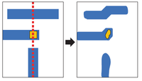
For 5nm node, the half-pitch is targeted at 11 nm.[181] For current 0.33 NA tools, at least two EUV exposures are required (see figure at left).
Single patterning extension
A return to extended generations of single exposure patterning would be possible with a wavelength even shorter than the 13.5 nm EUV wavelength or else higher numerical aperture (NA) tools. A much shorter wavelength (~6.7 nm) would be beyond EUV, and is often referred to as BEUV (Beyond Extreme UltraViolet).[182] Higher NA tools or different wavelengths would both pose new requirements for the multilayer optics. In particular, an NA of 0.45 using 13.5 nm wavelength already requires retuning of a few percent.[183] Increasing demagnification could avoid these issues, but the reduced field size severely affects large patterns (one die per 26 mm × 33 mm field) such as the many-core multi-billion transistor 14 nm Xeon chips.[184] A shorter wavelength would have worse shot noise effects without ensuring sufficient dose.[185]
In 2015, ASML disclosed details of its anamorphic next-generation EUV (13.5 nm wavelength) scanner, with an NA of 0.55. Its resolution was determined to be 12 nm, not quite the 11 nm half-pitch required for the 5 nm node. By comparison, its predecessor, the NXE:3300B with 0.33 NA, only has a resolution of 19 nm, not quite the 16 nm half-pitch required for the 7 nm node.[186] More seriously, the 0.55 NA has a much smaller depth of focus than immersion lithography.[187] Also, an anamorphic 0.52 NA tool has been found to exhibit too much CD and placement variability for 5 nm node single exposure and multi-patterning cutting.[188]
Depth of focus[189] being reduced by increasing NA is also a concern,[190] especially in comparison with multipatterning exposures using 193 nm immersion lithography:
| wavelength | refractive index | NA | DOF (normalized)[189] |
|---|---|---|---|
| 193 nm | 1.44 | 1.35 | 1 |
| 13.5 nm | 1 | 0.33 | 1.17 |
| 13.5 nm | 1 | 0.55 | 0.4 |
Resource requirements
| Utility | 200 W output EUV | 90 W output ArF immersion double patterning |
|---|---|---|
| Electrical power (kW) | 532 | 49 |
| Cooling water flow (L/min) | 1600 | 75 |
| Gas lines | 6 | 3 |
Source: Gigaphoton, Sematech Symposium Japan, September 15, 2010
The required utility resources are significantly larger for EUV compared to 193 nm immersion, even with two exposures using the latter. Hynix reported at the 2009 EUV Symposium that the wall plug efficiency was ~0.02% for EUV, i.e., to get 200 W at intermediate focus for 100 WPH, one would require 1 MW of input power, compared to 165 kW for an ArF immersion scanner, and that even at the same throughput, the footprint of the EUV scanner was ~3x the footprint of an ArF immersion scanner, resulting in productivity loss.[191] Additionally, to confine ion debris, a superconducting magnet may be required.[192]
Demonstrations

Interference lithography at the Paul Scherrer Institute[193] has been used to demonstrate sub-10 nm line-space features.[194][195] The resist performance tested with this source does not reflect the performance expected for an EUV projection tool due to the limited contrast of projection tools.
In 1996, a collaboration between Sandia National Laboratories, University of California at Berkeley, and Lucent Technologies, produced NMOS transistors with gate lengths from 75 nm to 180 nm. The gate lengths were defined by EUV lithography.[196] The device saturation current at 130 nm gate length was ~0.2 mA/um. A 100 nm gate device showed subthreshold swing of 90 mV/decade and saturated transconductance of 250 mS/mm. A commercial NMOS at the same design rule patterned by then-state-of-the-art DUV lithography[197] showed 0.94 mA/um saturation current and 860 mS/mm saturated transconductance. The subthreshold swing in this case was less than 90 mV/decade.
In February 2008, a collaboration including IBM and AMD, based at the College of Nanoscale Science and Engineering (CNSE) in Albany, New York, used EUV lithography to pattern 90 nm trenches in the first metal layer of a 45 nm node test chip.[198] No specific details on device performance were given.[199] However, the lithographic performance details given still indicated much to be desired:[200]
- CD uniformity: 6.6%
- Overlay: 17.9 nm x, 15.6 nm y, possibly correctable to 6.7 nm x, 5.9 nm y
- Power: 1 W at wafer (>200 W required for high volume), with a dose of 3.75 mJ/cm2
- Defects: 1/sq. cm.
The high defect level may not be unexpected as AMD's 45 nm node Metal 1 design rule was 90 nm while the same EUV exposure theoretically could result in printed defects below 30 nm originating from mask defects larger than 100 nm. Optical lithography pushed beyond its natural resolution limit has a significant advantage in this regard.
Apparently, the CNSE EUV tool suffered from a well-known 16% flare problem.[201] Flare effects may be difficult to separate from the secondary electron effects discussed earlier.
Also in July 2008, IMEC printed ~60 nm contacts using their installed EUV tool.[202] Doses of 12–18 mJ/cm2 were used.
In August 2008, SEMATECH demonstrated a 22 nm half-pitch using chemically-amplified photoresist. However, even at 15 mJ/cm2, the linewidth roughness was very significant, 5–6 nm, so that even the image pitch regularity was challenged.[203]
In April 2009, IMEC fabricated 22 nm SRAM cells where the contact and Metal 1 layers (~45 nm design rule) were printed with EUV lithography.[204] However, it was acknowledged that EUV would not be ready when companies start using 22 nm. In addition, it was commented that the feature edge profiles indicated slope asymmetry related to the characteristic EUV illumination asymmetry. Whereas this demonstration only focused on a limited number of ~45 nm features, Intel's shot noise calculation above for billions of features ~30 nm indicates difficult challenges ahead for manufacturing.
In late 2009, KLA-Tencor and GlobalFoundries along with Lawrence Berkeley National Labs published a paper[205] which showed the stochastic behavior of EUV-generated secondary electrons in EUV resists. In particular, 32 nm half-pitch trenches showed significant edge roughness, width roughness and critical dimension (CD) variability.[206] It may also explain the ~15 nm resist blur observed in an earlier study.[207]
In July 2015, IBM demonstrated a 7 nm node test chip that was fabricated using EUV lithography.[208] However, the 30 nm fin pitch was achieved with self-aligned patterning, implying the resolution of EUV was not sufficient at this time.
Device damage
MOSFETs made with Germanium showed large sensitivity to EUV doses, starting to degrade even at levels of 10–20 mJ/cm2.[209]
References
- ↑ Intel 7nm by 2019
- ↑ Globalfoundries EUV by 2020
- ↑ Samsung 7nm by 2020
- ↑ TSMC 5nm by 2020
- ↑ ASML - Many ways to shrink (Nov 2014)
- ↑ WSJ on ASML
- ↑ EUVL activities in South Korea (including Samsung and SKHynix)
- ↑ H. Oizumi et al., Proc. SPIE vol. 5751, 1147 (2005).
- ↑ K. Motai et al., Proc. SPIE vol. 6517, 65170F (2007).
- ↑ Y. Nagaoka and J. Miyazaki, Proc. SPIE vol. 9635, 963510 (2015).
- 1 2 N. Felix et al., Proc. SPIE vol. 9776, 97761O (2015).
- ↑ C. Higgins et al., Proc. SPIE vol. 9048, 90481Q (2014).
- 1 2 P. De Bisschop et al., Proc. SPIE vol. 9048, 904809 (2014).
- ↑ P. De Bisschop et al., Proc. SPIE vol. 7973, 79730B (2011).
- 1 2 3 E. van Setten et al., Proc. SPIE 9231, 923108 (2014).
- ↑ J. van Schoot et al., Proc. SPIE 9422, 94221F (2015).
- ↑ Mark Winter. "WebElements Periodic Table of the Elements". webelements.com.
- ↑ Tao, Y.; et al. (2005). "Characterization of density profile of laser-produced Sn plasma for 13.5 nm extreme ultraviolet source". Appl. Phys. Lett. 86 (20): 201501. doi:10.1063/1.1931825.
- ↑ Sn vs. Xe ions as EUV light source
- ↑ Coons, R. W.; et al. (2010). "Comparison of EUV spectral and ion emission features from laser-produced Sn and Li plasmas". Proc. SPIE. 7636: 763636. doi:10.1117/12.848318.
- ↑ Paetzel, R.; et al. (2003). "Excimer lasers for superhigh NA 193-nm lithography". Proc. SPIE. 5040: 1665. doi:10.1117/12.485344.
- ↑ Harilal, S. S.; et al. (2006). "Spectral control of emissions from tin doped targets for extreme ultraviolet lithography". J. Phys. D. 39 (3): 484. doi:10.1088/0022-3727/39/3/010.
- ↑ Trintchouk, F.; et al. (2006). "XLA-300: the fourth-generation ArF MOPA light source for immersion lithography". Proc. SPIE. 6154: 615423. doi:10.1117/12.658723.
- ↑ V. Bakshi, 2009 EUVL Workshop Summary, Sheraton Waikiki, Hawaii, July 13–17, 2009.
- ↑ Cymer presentation at 2007 EUV Source Workshop
- ↑ Saleh, B. E. A.; Teich, M. C. (1991). "Fundamentals of Photonics". New York: John Wiley & Sons: 521. ISBN 0471839655.
- ↑ T. Asayama et al., Proc. SPIE vol. 8683, 86831G (2013).
- ↑ ASML update Nov. 2013, Dublin
- ↑ "A New Light Source for EUV Lithography". ieee.org.
- ↑ Chen, F. T. (2003). "Asymmetry and thickness effects in reflective EUV masks". Proc. SPIE. 5037: 347. doi:10.1117/12.483602.
- ↑ ASML update on ADT
- ↑ Gullikson, E. M.; et al. (1996). "Stable silicon photodiodes for absolute intensity measurements in the VUV and soft X-ray regions" (PDF). J. Electron Spec. and Rel. Phenom. 80: 313–316. doi:10.1016/0368-2048(96)02983-0.
- ↑ Keister, J. W. (2007). "Silicon Photodiodes for Absolute Soft X-ray Radiometry" (PDF). Proc. SPIE. 6689: 26. doi:10.1117/12.741601.
- ↑ Berger, K. W.; Campiotti, R. H. (2000). "Absolute dosimetry for extreme-ultraviolet lithography". Proc. SPIE. 3998: 838. doi:10.1117/12.386448.
- ↑ Donati, S. (2000). Photodetectors: Devices, Circuits and Applications. Upper Saddle River, NJ: Prentice-Hall PTR. p. 182. ISBN 0130203378.
- ↑ Robert W. Hamm and Marianne E. Hamm, "The Beam Business: Accelerators in Industry", Physics Today, June 2011, pp. 49–50
- ↑ "Intel, TSMC Revive EUV Hopes". EETimes.
- ↑ http://www.dvhardware.net/article62846.html. Missing or empty
|title=(help) - ↑ H. Komori et al., Proc. SPIE 5374, pp. 839–846 (2004).
- ↑ B. A. M. Hansson et al., Proc. SPIE 4688, pp. 102–109 (2002).
- ↑ S. N. Srivastava et al., J. Appl. Phys.' 102, 023301 (2007).
- ↑ L. Peters, "Double Patterning Leads Race for 32 nm", Semiconductor International, October 18, 2007.
- ↑ M. Sugawara et al., J. Vac. Sci. Tech. B 21, 2701 (2003).
- ↑ M. Chandhok et al., J. Vac. Sci. Tech B 22, 2966 (2004).
- ↑ EUV uptime still an issue.
- ↑ S. Jeong et al., Proc. SPIE 3997, 431 (2000).
- ↑ I-S. Kim et al., Proc. SPIE vol. 8322, 83222X (2012).
- ↑ N. S. Faradzhev et al., Bull. of the Russ. Acad. of Sci., Physics, vol. 74, pp. 28–32 (2010).
- ↑ F. Barkusky et al., Optics Express 18, 4346 (2010).
- ↑ M. Muller et al., Appl. Phys. A 108, 263 (2012).
- ↑ A. R. Khorsand et al., Optics Express vol. 18, 700 (2010).
- ↑ J. V. Hermans et al., Proc. SPIE 7969, 79691M (2011).
- ↑ D. Tretheway and E. S. Aydil, J. Electrochem. Soc., vol. 143, 3674 (1996).
- ↑ M. S. Bakir et al., CICC 2007, 421 (2007).
- ↑ J. A. van der Pol et al., Microelectronics Rel., 39, 863 (1999).
- ↑ "J. Mathuni et al., Wafer Backside Paper" (PDF). seconsemi.com.
- ↑ Brewer Science LED Brochure featuring Substrate Protection
- ↑ "ASML: Products - TWINSCAN NXE:3300B". asml.com.
- 1 2 X. Liu et al., Proc. SPIE vol. 9048, 90480Q (2014).
- ↑ T. Schmoeller et al., Proc. SPIE vol. 6921, 69211B (2008).
- ↑ P. Liu et al., Proc. SPIE vol. 8679, 86790W (2013).
- ↑ EUV Mask Flatness Requirements
- ↑ B. L. Henke et al., J. Appl. Phys. 48, pp. 1852–1866 (1977).
- ↑ SPIE EUV08 paper by T. Kozawa and S. Tagawa
- ↑ N. Shimizu and H. Sato, 1996 IEEE Annual Report - Conference on Electrical Insulation and Dielectric Phenomena, pp. 787–790 (1996)
- ↑ Y. Ekinci et al., Microelectronic Engineering, vol. 84, pp. 700–704 (2007). Conference draft.
- ↑ T. Kozawa et al., J. Vac. Sci. Tech. B 15, pp. 2582–2586 (1997).
- ↑ T. Kozawa et al., J. Vac. Sci. Tech. B 22, pp. 3489–3492 (2004).
- ↑ E. Stoffels et al., Plasma Sources Sci. & Tech. 10, 311-317 (2001).
- ↑ M. P. Seah and W. A. Dench, Surf. Interf. Anal. 1, 2-11 (1979).
- ↑ S. Tanuma et al., Surf. Interf. Anal. 21, 165–176 (1993).
- ↑ B. Yakshinskiy et al., Intl. Symp. on EUVL 2009
- ↑ C. Song et al., Chem. Mater. 20, 3473–3479 (2008).
- ↑ H. H. Solak et al., Microel. Eng. 67–68, pp. 56–62 (2003).
- ↑ J. M. Roberts et al., Proc. SPIE 7273, 72731W (2009).
- ↑ T. Kozawa et al., Appl. Phys. Exp. 1, 027001 (2008).
- ↑ T. Watanabe and H. Kinoshita, J. Photopolymer Sci. and Tech., vol. 21, 777–784 (2008).
- ↑ R. Gronheid et al., J. Micro/Nanolith. MEMS MOEMS 10, 033004 (2011).
- ↑ A. Ritucci et al., "Damage and ablation of large band gap dielectrics induced by a 46.9 nm laser beam," March 9, 2006 report UCRL-JRNL-219656 (Lawrence Livermore National Laboratory).
- ↑ G. Denbeaux et al., 2007 European Mask and Lithography Conference.
- ↑ I. Pollentier et al., Proc. SPIE vol. 7972, 797208 (2011).
- ↑ G. Denbeaux, 2009 Intl. Workshop on EUV Lithography.
- ↑ J. Y. Park et al., J. Vac. Sci. Tech. B29, 041602 (2011).
- ↑ C. A. Cutler et al., Proc. SPIE vol. 5037, 406 (2003).
- ↑ D. Lauvernier et al., Microelectonic Eng. 75, 177–182 (2004).
- ↑ E. W. Scheckler et al., J. Vac. Sci. Tech. B 12, 2361 (1994).
- ↑ N. Koch et al., Thin Solid Films 391, pp. 81–87 (2001).
- ↑ J. Hollenshead and L. Klebanoff, J. Vac. Sci. & Tech. B 24, pp. 118–130 (2006).
- ↑ J. Hollenshead and L. Klebanoff, J. Vac. Sci. & Tech. B 24, pp. 64–82 (2006).
- ↑ M. H. L. van der Velden et al., J. Appl. Phys. 100, 073303 (2006).
- ↑ "Getting up to speed with roadmap requirements for extreme-UV lithography". spie.org.
- ↑ H. Yu et al., J. Vac. Sci. Tech. A31, 021403 (2013).
- ↑ "Fast Simulation Methods for Non-Planar Phase and Multilayer Defects in DUV and EUV Photomasks for Lithography". berkeley.edu.
- ↑ P. P. Naulleau et al., Optics Communications 200, pp. 27–34 (2001).
- ↑ S. Huh et al., Proc. SPIE 7271 (2009).
- ↑ K. Seki et al., Proc. SPIE 9658, 96580G (2015).
- ↑ A. Garetto et al., J. Micro/Nanolith. MEMS MOEMS 13, 043006 (2014).
- ↑ C. Zoldeski et al., Proc. SPIE vol. 9048, 90481N (2014).
- ↑ D. L. Goldfarb, Dec. 2015 BACUS Newsletter.
- ↑ A. Gao et al., J. Appl. Phys. 114, 044313 (2013).
- ↑ E. Gallagher et al., Proc. SPIE vol. 9635, 96350X (2015).
- ↑ C. Ghica et al., Rom. Rep. in Phys., vol. 62, 329-340 (2010).
- ↑ L. Juan et al., Chin. Phys. B, vol., 22, 105101 (2013).
- ↑ B. McClinton, Ph.D. Thesis, U. C. Berkeley, 2011.
- ↑ R. Petit et al., Electromagnetic Theory of Gratings, Springer-Verlag, 1980.
- ↑ K. Murakami et al., Proc. SPIE 8322, 832215 (2012).
- ↑ K. Bubke et al., Proc. SPIE vol. 6283, 628318 (2006).
- ↑ J. T. Neumann et al., May 2013 BACUS Newsletter
- ↑ M. A. Golub and A. A. Friesem, J. Opt. Soc. Am. A, 24, 687 (2007).
- ↑ Louis, E.; et al. (2011). "Nanometer interface and materials control for multilayer EUV-optical applications". Prog. Surf. Sci. 86 (11–12): 255–294. doi:10.1016/j.progsurf.2011.08.001.
- ↑ C.-H. Lin et al., Microel. Eng. 84, 711 (2007).
- ↑ A. Erdmann et al., Proc. SPIE vol. 8679, 86791Q (2013).
- ↑ K. Takai et al., Proc. SPIE vol. 9235, 923515 (2014).
- ↑ N. Davydova et al., Proc. SPIE vol. 7985, 79850X (2011).
- ↑ N. Davydova et al., Proc. SPIE vol. 8166, 816624 (2011).
- ↑ E. van Setten et al., Proc. SPIE vol. 7823, 78231O (2010).
- ↑ N. Davydova et al., Proc. SPIE vol. 8880, 888027(2013).
- ↑ "5nm Fab Challenges". 2016-01-20.
ASML is developing an anamorphic lens for EUV. The two-axis EUV lens would support 8x magnification in the scan mode and 4x in the other direction. It would support 0.5 to 0.6 NAs. … The EUV scanner could take a throughput hit. It would expose the wafer at only half the field size, as opposed to full field sizes with today’s EUV scanners.
- ↑ Hilbert Hagedoorn. "GeForce GTX 780 review". Guru3D.com.
- ↑ Intel Xeon E5-2600 v3
- ↑ J. T. Neumann et al., Proc. SPIE vol. 8522, 852211 (2012).
- ↑ K. Takehisa, Proc. SPIE vol. 8701, 87010T (2013).
- ↑ J. Zimmerman, Mask TWG, EUVL 2008 Symposium.
- ↑ B. Baylav, "Reduction of Line Edge Roughness (LER) in Interference-Like Large Field Lithography", PhD dissertation, p. 37, 2014.
- ↑ D. C. Brandt et al., Proc. SPIE vol. 7271, 727103 (2009).
- ↑ F. T. Chen et al., Proc. SPIE 8326, 8326L (2012).
- ↑ 2013 Nissan Chemical Industries, 2013 International Workshop on EUV Lithography
- ↑ T. G. Oyama et al., Appl. Phys. Exp. 7, 036501 (2014).
- ↑ T. Kozawa, Jap. J. Appl. Phys. 51, 06FC01 (2012).
- 1 2 E. van Setten et al., Proc. SPIE 9661, 96610G (2015).
- ↑ S. Hsu et al., Proc. SPIE vol. 9422, 94221I (2015).
- ↑ Z-Y. Pan et al., Proc. SPIE vol. 6924, 69241K (2008).
- ↑ D. Mamezaki et al., J. Photopolym. Sci & Tech. 29, 749 (2016).
- ↑ J. Torok et al., J. Photopolym. Sci. Tech. vol. 26, 625 (2013).
- ↑ J. W. Thackeray et al., J. Photopolym. Sci. & Tech., 23, 631 (2010).
- ↑ H.-J. Cho et al., 2016 Symposium on VLSI Technology Digest of Technical Papers, 12.
- ↑ p.53
- ↑ G. Denbeaux et al., 2013 International Workshop on EUV Lithography.
- ↑ J. Torok et al., J. Photopolymer Sci. & Tech., 27, 611 (2014).
- ↑ A. Narasimhan et al., Proc. SPIE vol. 9422, 942208 (2015).
- 1 2
- ↑
- ↑
- ↑
- ↑
- ↑
- ↑
- ↑
- ↑ ASML. "ASML reports 2013 results". US Securities and Exchange Commission. Retrieved 2014-07-16.
We remain on target to deliver EUV systems with a throughput of 70 wafers per hour in 2014, upgradeable to 125 wafers per hour in 2015.
- 1 2 ASML. "Investor Day London". US Securities and Exchange Commission. Retrieved 2014-11-28.
- ↑ "ASML: Press - Press Releases - ASML Announces New High Mark for EUV Productivity; TSMC Images More Than 1000 Wafers in a Single Day". asml.com.
- ↑ "ASML 2015 Third Quarter Results".
- ↑ Tiernan Ray. "ASML Gets a Lift From TSM, Though Questions on EUV Remain". Barrons.
- 1 2 "ASML 2015 Fourth Quarter and 2015 Annual Results".
- 1 2 "ASML Holding's (ASML) CEO Peter Wennink on Q4 2015 Results - Earnings Call Transcript".
- 1 2 3 "ASML 2015 Second Quarter Results".
- ↑
- ↑ (PDF) http://brion.com/wordpress/wp-content/uploads/2010/08/Holistic-lithography-for-EUV.pdf. Missing or empty
|title=(help) - ↑ . 2012-04-18 http://optics.org/news/3/4/23. Missing or empty
|title=(help) - ↑ R. Peeters et al., Proc. SPIE 9048, 90481J (2014).
- ↑ "ASML confident of 2016 EUV goals; Dutch lithography giant expects to ship at least six systems as customers target 2018 production ramp". 2016-01-20.
- ↑ A. Pirati et al., Proc. SPIE 9776, 97760A (2015).
- ↑ ASML reports early 2016 results
- ↑ 2016 EUV Mask Pellicle TWG update
- ↑ F. Jiang et al., Proc. SPIE vol. 9422, 94220U (2015).
- ↑ IBM Expert on lithography for 7 nm ICs.
- ↑ A. Chen, EUV exposure systems for volume production, SEMATECH Symposium Taiwan 2010.
- ↑ G-J.Kim et al., J. Micro/Nanolith. MEMS MOEMS 15, 023503 (2016).
- ↑ J. Mulkens et al., Proc. SPIE 9048, 90481L (2014).
- ↑ A-Y. Je et al., Proc. SPIE 7823, 78230Z (2010).
- ↑ T. Huynh-Bao et al., Proc. SPIE 9781, 978102 (2016).
- ↑ Intel presentation on Complementary Lithography at 2012 International Workshop on EUV Lithography
- ↑ F. T. Chen et al., Proc. SPIE vol. 8683, 868311 (2013).
- ↑ S. Owa et al., Proc. SPIE vol. 9052, 90520O (2014).
- ↑ "Semiconductor roadmapping update: Front-end technologies – Part 2". electroiq.com.
- ↑ E. van Setten et al., Proc. SPIE vol. 8352, 835205 (2012).
- ↑ ASML presentation at 2013 Semicon West
- ↑ ITRS 2012 Litho One Pager April 24, 2012
- ↑ B. J. Lin, Proc. SPIE vol. 9426, 942602 (2015).
- ↑ W. Gillijns et al., Proc. SPIE vol. 9427, 942709 (2015).
- ↑ B. J. Lin, Microelec. Eng. 143, 91–101 (2015).
- ↑ ASML presentation at 2010 International Workshop on Extreme Ultraviolet Sources
- ↑ J. T. Neumann et al., Proc. SPIE 8522, 852211 (2012).
- ↑ Intel’s Xeon E5-2600 V4 Chips Feature An Insane 7.2 Billion Transistors on a 456mm2 Die
- ↑ N. Mojarad et al., Sci. Rep. 5, 9235 (2015).
- ↑ J. van Schoot et al., Proc. SPIE vol. 9422, 94221F (2015).
- ↑ B. J. Lin, JM3 1, 7–12 (2002).
- ↑ E. R. Hosler et al., Proc. SPIE vol. 9776, 977616 (2015).
- 1 2 B. J. Lin, J. Microlith., Microfab., Microsyst. 1, 7-12 (2002).
- ↑ B. J. Lin, Microelec. Eng. 143, 91-101 (2015).
- ↑ H. S. Kim, Future of Memory Devices and EUV Lithography, 2009 EUV Symposium
- ↑ H. Mizoguchi, "Laser Produced Plasma EUV Light Source Gigaphoton Update," EUVL Source Workshop, May 12, 2008.
- ↑ "Paul Scherrer Institut (PSI) ::". psi.ch.
- ↑ XIL beamline at PSI
- ↑ V. Auzelyte et al., J. Micro/Nanolith. MEMS MOEMS 8, 021204 (2009).
- ↑ K. B. Nguyen et al., J. Vac. Sci. Tech. B 14, 4188 (1996).
- ↑ S. Yang et al., IEDM '98 Technical Digest, pp. 197–200 (1998).
- ↑ B. La Fontaine et al., Proc. SPIE 6921, 69210P (2008).
- ↑ Wolfgang Gruener. "AMD reports successful production of full-field EUV test chip". TG Daily.
- ↑ "Semiconductors". pennnet.com.
- ↑ O. R. Wood II et al., Proc. SPIE 6517, 65170U (2007).
- ↑ "IMEC reports major progress in EUV". physorg.com.
- ↑ Semiconductor International: Sematech EUV Resist at 22 nm Half-Pitch
- ↑ IMEC Makes 22 nm SRAM Cells With EUV Lithography
- ↑ J. J. Biafore et al., SPIE Lithography Asia 2009, Proc. SPIE 7520, 75201P (2009).
- ↑ "KLA-Tencor brings stochastic modeling to virtual tool for EUV, DPL". electroiq.com.
- ↑ T. I. Wallow et al., Proc. SPIE 7273, 72733T (2009).
- ↑ IBM leapfrogs Intel to 7 nm
- ↑ Y-T. Chen et al., IEEE Elec. Dev. Lett., vol. 34, 1220 (2013).
Further reading
- Banqiu Wu and Ajay Kumar (May 2009). Extreme Ultraviolet Lithography. McGraw-Hill Professional, Inc. ISBN 0-07-154918-8.
- Banqiu Wu and Ajay Kumar (2009). "Extreme Ultraviolet Lithography: Towards the Next Generation of Integrated Circuits". Optics & Photonics Focus. 7 (4).
Related links
| Main | ||
|---|---|---|
| Other | ||
| See also | ||