Electron holography
Electron holography is holography with electron waves. Dennis Gabor invented holography in 1948[1] when he tried to improve resolution in electron microscope. The first attempts to perform holography with electron waves were made by Haine and Mulvey in 1952;[2] they recorded holograms of zinc oxide crystals with 60keV electrons, demonstrating reconstructions with approximately 1 nm resolution. In 1955 G. Möllenstedt and H. Düker[3] invented an electron biprism. thus enabling the recording of electron holograms in off-axis scheme. There are many different possible configurations for electron holography, with more than 20 documented in 1992 by Cowley. [4] Usually, high spatial and temporal coherence (i.e. a low energy spread) of the electron beam are required to perform holographic measurements.
High-energy electron holography in off-axis scheme
Electron holography with high-energy electrons (80-200keV) can be realized in a transmission electron microscope (TEM) in an off-axis scheme. Electron beam is split into two parts by very thin positively charged wire. Positive voltage deflects the electron waves so that they overlap and produce an interference pattern of equidistantly spaced fringes.
Reconstruction of off-axis holograms is done numerically and it consists of two mathematical transformations.[5] First, a Fourier transform of the hologram is performed. The resulting complex image consists of the autocorrelation (center band) and two mutually conjugated sidebands. Only one side band is selected by applying a low-pass filter (round mask) centered on the chosen side-band. The central band and the twin side-band are both set to zero. Next, the selected side-band is re-positioned to the center of the complex image and the backward Fourier-transform is applied. The resulting image in the object domain is complex-valued, and thus, the amplitude and phase distributions of the object function are reconstructed.
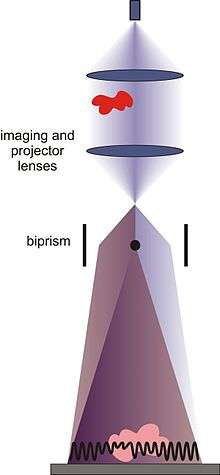
Electron holography in in-line scheme
Original holographic scheme by Dennis Gabor is inline scheme, which means that reference and object wave share the same optical axis. This scheme is also called point projection holography. An object is placed into divergent electron beam, part of the wave is scattered by the object (object wave) and it interferes with the unscattered wave (reference wave) in detector plane. The spatial coherence in in-line scheme is defined by the size of the electron source. Holography with low-energy electrons (50-1000eV) can be realized in in-line scheme.[6]

Electromagnetic fields
It is important to shield the interferometric system from electromagnetic fields, as they can induce unwanted phase-shifts due to the Aharonov–Bohm effect. Static fields will result in a fixed shift of the interference pattern. It is clear every component and sample must be properly grounded and shielded from outside noise.
Applications
Electron holography[7][8] is commonly used to study electric and magnetic fields in thin films, as magnetic and electric fields can shift the phase of the interfering wave passing through the sample.[9]
The principle of electron holography can also be applied to interference lithography.[10]
References
- ↑ D. Gabor, A new microscopic principle, Nature 4098, 777 (1948).
- ↑ M. E. Haine, T. Mulvey, The formation of the diffraction image with electrons in the Gabor diffraction microscope, J. Opt. Soc. Am. 42, 763 (1952).
- ↑ G. Möllenstedt and H. Düker, Beobachtungen und Messungen an Biprisma-Interferenzen mit Elektronenwellen, Zeitschrift für Physik, 145, 377 (1956).
- ↑ J. M. Cowley, Twenty forms of electron holography, Ultramicroscopy 41, 335–348 (1992).
- ↑ M. Lehmann, H. Lichte, Tutorial on off-axis electron holography, Microsc. Microanal. 8(6), 447–466 (2002).
- ↑ H.-W. Fink, W. Stocker and H. Schmid, Holography with low-energy electrons, Phys. Rev. Lett. 65(10), 1204–1206 (1990).
- ↑ H. Lichte, Electron holography approaching atomic resolution, Ultramicroscopy 20, 293 (1986).
- ↑ A. Tonomura, Applications of electron holography, Rev. Mod. Phys. 59, 639 (1987).
- ↑ R. E. Dunin-Borkowski et al., Micros. Res. and Tech. 64, 390 (2004).
- ↑ K. Ogai et al., Jpn. J. Appl. Phys. 32, 5988 (1993).