Xeon
 | |
| Produced | From 1998 to present |
|---|---|
| Common manufacturer(s) |
|
| Max. CPU clock rate | 1.2 GHz to 4.4 GHz |
| FSB speeds | 600 MHz to 8.0 GT/s |
| Instruction set | x86-64 |
| Microarchitecture | Skylake, Broadwell, Haswell, Ivy Bridge, Sandy Bridge, Nehalem, Core, NetBurst, P6 |
| Cores |
Up to 72, over 200 when used with dual Xeon Phi co-processors |
| Socket(s) |
|
The Xeon /ˈziːɒn/ is a brand of x86 microprocessors designed, manufactured, and marketed by Intel Corporation, targeted at the non-consumer workstation, server, and embedded system markets. The primary advantages of the Xeon CPUs, when compared to the majority of Intel's desktop-grade consumer CPUs, are their multi-socket capabilities, higher core counts, and support for ECC memory. A Xeon Phi co-processor, or co-processors, can be used alongside an existing Intel Xeon processor to provide increased/improved computing power, requiring an available PCI Express 3.0 x16 slot in x16, or x8 mode. Intel Xeon CPUs support the following chipsets: Z87, X99, and for dual CPUs the C600 series of chipsets.
Disadvantages that make Xeon processors unsuitable for most consumer-grade desktop PCs include lower clock rates at the same price point (since servers run more tasks in parallel than desktops), absence of an integrated GPU, and non-existent support for overclocking. Despite such disadvantages, Xeon processors have always had popularity among desktop users, (primarily gamers, and extreme users) mainly due to higher core count potential, and higher price to performance ratio vs. the Core i7. Because most Intel Xeon CPUs lack an integrated GPU, systems built with such integrated GPU lacking processors require a discrete graphics card if a VDU output is desired.[1]
Overview
The Xeon brand has been maintained over several generations of x86 and x86-64 processors. Older models added the Xeon moniker to the end of the name of their corresponding desktop processor, but more recent models used the name Xeon on its own. The Xeon CPUs generally have more cache than their desktop counterparts in addition to multiprocessing capabilities.
| Intel Xeon processor family | |||||
|---|---|---|---|---|---|
| Server – (UP/DP) 3000/5000/E3/E5-1xxx and 2xxx/E7-2xxx series | Server – (MP) 7000/E5-4xxx/E7-4xxx and 8xxx series | ||||
| Code-named | Core | Date released | Code-named | Core | Date released |
| Drake | (250 nm) | Jun 1998 | |||
| Tanner Cascades |
(250 nm) (180 nm) |
Mar 1999 Oct 1999 | |||
| Foster Prestonia Gallatin Nocona Irwindale Paxville Dempsey |
(180 nm) (130 nm) (130 nm) (90 nm) (90 nm) dual (90 nm) dual (65 nm) |
May 2001 Feb 2002 Mar 2003 Jun 2004 Feb 2005 Oct 2005 May 2006 |
Foster MP Gallatin MP Cranford Potomac Paxville MP Tulsa |
(180 nm) (130 nm) (90 nm) (90 nm) dual (90 nm) dual (65 nm) |
Mar 2002 Nov 2002 Mar 2005 Mar 2005 Dec 2005 Aug 2006 |
| Sossaman Woodcrest Conroe Allendale Wolfdale Kentsfield Yorkfield Wolfdale DP Clovertown Harpertown |
dual (65 nm) dual (65 nm) dual (65 nm) dual (65 nm) dual (45 nm) quad (65 nm) quad (45 nm) dual (45 nm) quad (65 nm) quad (45 nm) |
Mar 2006 Jun 2006 Oct 2006 Jan 2007 Feb 2008 Jan 2007 Mar 2008 Nov 2007 Nov 2006 Nov 2007 |
Tigerton Dunnington Dunnington |
dual (65 nm) quad (45 nm) six (45 nm) |
Sep 2007 Sep 2008 Sep 2008 |
| Nehalem-EP Bloomfield Beckton (65xx) Westmere-EX (E7-2xxx) Sandy Bridge-EP Ivy Bridge (E3 v2/E5-1xxx/2xxx v2) Ivy Bridge-EX (E7-28xx v2) Haswell (E3 v3/E5-1xxx/2xxx v3) Broadwell (E3 v4/E5-1xxx/2xxx v4) Skylake-DT (E3 v5) |
dual/quad (45 nm) quad (45 nm) quad/six/eight (45 nm) six/eight/ten (32 nm) dual/quad/six/eight (32 nm) dual/quad/six/eight/ten/twelve (22 nm) twelve/fifteen (22 nm) 2/4/6/8/10/12/14/16/18 (22 nm) 4/6/8/10/12/14/16/18/20/22 (14 nm) quad (14 nm) |
Mar 2009 Mar 2009 Mar 2010 Apr 2011 Mar 2012 Sep 2013 Feb 2014 Sep 2014 Jun 2015 Oct 2015 |
Beckton (75xx) Westmere-EX (E7-4xxx/8xxx) Sandy Bridge-EP (E5-46xx) Ivy Bridge-EP (E5-46xx v2) Ivy Bridge-EX (E7-48xx/88xx v2) Haswell-EP (E5-46xx v3) Haswell-EX (E7-48xx/88xx v3) |
quad/six/eight (45 nm) six/eight/ten (32 nm) quad/six/eight (32 nm) quad/six/eight/ten/twelve (22 nm) six/eight/ten/twelve/fifteen (22 nm) 6/10/12/14/16/18 (22 nm) 4/8/10/12/14/16/18 (22 nm) |
Mar 2010 Apr 2011 May 2012 March 2014 Feb 2014 Jun 2015 May 2015 |
| List of Intel Xeon microprocessors | |||||
P6-based Xeon
Pentium II Xeon
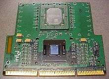
The first Xeon-branded processor was the Pentium II Xeon (code-named "Drake"). It was released in 1998, replacing the Pentium Pro in Intel's server lineup. The Pentium II Xeon was a "Deschutes" Pentium II (and shared the same product code: 80523) with a full-speed 512 kB, 1 MB, or 2 MB L2 cache. The L2 cache was implemented with custom 512 kB SRAMs developed by Intel. The number of SRAMs depended on the amount of cache. A 512 kB configuration required one SRAM, a 1 MB configuration: two SRAMs, and a 2 MB configuration: four SRAMs on both sides of the PCB. Each SRAM was a 12.90 mm by 17.23 mm (222.21 mm²) die fabricated in a 0.35 µm four-layer metal CMOS process and packaged in a cavity-down wire-bonded land grid array (LGA).[2] The additional cache required a larger module and thus the Pentium II Xeon used a larger slot, Slot 2. It was supported by the 440GX dual-processor workstation chipset and the 450NX quad- or octo-processor chipset.
Pentium III Xeon
In 1999, the Pentium II Xeon was replaced by the Pentium III Xeon. Reflecting the incremental changes from the Pentium II "Deschutes" core to the Pentium III "Katmai" core, the first Pentium III Xeon, named "Tanner", was just like its predecessor except for the addition of Streaming SIMD Extensions (SSE) and a few cache controller improvements. The product codes for Tanner mirrored that of Katmai; 80525.
The second version, named "Cascades", was based on the Pentium III "Coppermine" core. The "Cascades" Xeon used a 133 MHz bus and relatively small 256 kB on-die L2 cache resulting in almost the same capabilities as the Slot 1 Coppermine processors, which were capable of dual-processor operation but not quad-processor operation.
To improve this situation, Intel released another version, officially also named "Cascades", but often referred to as "Cascades 2 MB". That came in two variants: with 1 MB or 2 MB of L2 cache. Its bus speed was fixed at 100 MHz, though in practice the cache was able to offset this. The product code for Cascades mirrored that of Coppermine; 80526.
Netburst-based Xeon
Xeon (DP) & Xeon MP (32-bit)
Foster
In mid-2001, the Xeon brand was introduced ("Pentium" was dropped from the name). The initial variant that used the new NetBurst microarchitecture, "Foster", was slightly different from the desktop Pentium 4 ("Willamette"). It was a decent chip for workstations, but for server applications it was almost always outperformed by the older Cascades cores with a 2 MB L2 cache and AMD's Athlon MP. Combined with the need to use expensive Rambus Dynamic RAM, the Foster's sales were somewhat unimpressive.
At most two Foster processors could be accommodated in a symmetric multiprocessing (SMP) system built with a mainstream chipset, so a second version (Foster MP) was introduced with a 1 MB L3 cache and the Jackson Hyper-Threading capacity. This improved performance slightly, but not enough to lift it out of third place. It was also priced much higher than the dual-processor (DP) versions. The Foster shared the 80528 product code with Willamette.
Prestonia
In 2002 Intel released a 130 nm version of Xeon branded CPU, codenamed "Prestonia". It supported Intel's new Hyper-Threading technology and had a 512 kB L2 cache. This was based on the "Northwood" Pentium 4 core. A new server chipset, E7500 (which allowed the use of dual-channel DDR SDRAM), was released to support this processor in servers, and soon the bus speed was boosted to 533 MT/s (accompanied by new chipsets: the E7501 for servers and the E7505 for workstations). The Prestonia performed much better than its predecessor and noticeably better than Athlon MP. The support of new features in the E75xx series also gave it a key advantage over the Pentium III Xeon and Athlon MP branded CPUs (both stuck with rather old chipsets), and it quickly became the top-selling server/workstation processor.
"Gallatin"
%2C_Socket_604.jpg) | |
| Produced | From March 2003 to 2004 |
|---|---|
| Max. CPU clock rate | 1.5 GHz to 3.2 GHz |
| FSB speeds | 400 MT/s to 533 MT/s |
| Min. feature size | 130 nm |
| Instruction set | x86 |
| Microarchitecture | NetBurst |
| CPUID code | 0F7x |
| Product code | 80537 |
| Cores | 1 |
| L1 cache | 8 kB + 12 kuOps trace cache |
| L2 cache | 512 kB |
| L3 cache | 1 MB, 2 MB, 4 MB |
| Application | DP and MP Server |
| Package(s) | |
| Brand name(s) |
|
Subsequent to the Prestonia was the "Gallatin", which had an L3 cache of 1 MB or 2 MB. Its Xeon MP version also performed much better than the Foster MP, and was popular in servers. Later experience with the 130 nm process allowed Intel to create the Xeon MP branded Gallatin with 4 MB cache. The Xeon branded Prestonia and Gallatin were designated 80532, like Northwood.
Xeon (DP) & Xeon MP (64-bit)
Nocona and Irwindale
Due to a lack of success with Intel's Itanium and Itanium 2 processors, AMD was able to introduce x86-64, a 64-bit extension to the x86 architecture. Intel followed suit by including Intel 64 (formerly EM64T; it is almost identical to AMD64) in the 90 nm version of the Pentium 4 ("Prescott"), and a Xeon version codenamed "Nocona" with 1 MB L2 cache was released in 2004. Released with it were the E7525 (workstation), E7520 and E7320 (both server) chipsets, which added support for PCI Express, DDR-II and Serial ATA. The Xeon was noticeably slower than AMD's Opteron, although it could be faster in situations where Hyper-Threading came into play.
A slightly updated core called "Irwindale" was released in early 2005, with 2 MB L2 cache and the ability to have its clock speed reduced during low processor demand. Although it was a bit more competitive than the Nocona had been, independent tests showed that AMD's Opteron still outperformed Irwindale. Both of these Prescott-derived Xeons have the product code 80546.
Cranford and Potomac
64-bit Xeon MPs were introduced in April 2005. The cheaper "Cranford" was an MP version of Nocona, while the more expensive "Potomac" was a Cranford with 8 MB of L3 cache. Like Nocona and Irwindale, they also have product code 80546.
Dual-Core Xeon
"Paxville DP"
| Produced | From October 2005 to August 2008 |
|---|---|
| Max. CPU clock rate | 2667 MHz to 3000 MHz |
| FSB speeds | 667 MT/s to 800 MT/s |
| Min. feature size | 90 nm |
| Instruction set | x86 |
| Microarchitecture | NetBurst |
| CPUID code | 0F48 |
| Product code | 80551, 80560 |
| Cores | 2 |
| L2 cache | 2×2 MB |
| Application | DP Server, MP Server |
| Package(s) | |
| Brand name(s) |
|
The first dual-core CPU branded Xeon, codenamed Paxville DP, product code 80551, was released by Intel on 10 October 2005. Paxville DP had NetBurst microarchitecture, and was a dual-core equivalent of the single-core Irwindale (related to the Pentium D branded "Smithfield") with 4 MB of L2 Cache (2 MB per core). The only Paxville DP model released ran at 2.8 GHz, featured an 800 MT/s front side bus, and was produced using a 90 nm process.
7000-series "Paxville MP"
An MP-capable version of Paxville DP, codenamed Paxville MP, product code 80560, was released on 1 November 2005. There are two versions: one with 2 MB of L2 Cache (1 MB per core), and one with 4 MB of L2 (2 MB per core). Paxville MP, called the dual-core Xeon 7000-series, was produced using a 90 nm process. Paxville MP clock ranges between 2.67 GHz and 3.0 GHz (model numbers 7020–7041), with some models having a 667 MT/s FSB, and others having an 800 MT/s FSB.
| Model | Clock Frequency (GHz) | L2 Cache (MB) | FSB (MHz) | TDP (W) |
|---|---|---|---|---|
| 7020 | 2.66 | 2 × 1 | 667 | 165 |
| 7030 | 2.80 | 2 × 1 | 800 | 165 |
| 7040 | 3.00 | 2 × 2 | 667 | 165 |
| 7041 | 3.00 | 2 × 2 | 800 | 165 |
7100-series "Tulsa"
| Produced | From August 2006 to August 2008 |
|---|---|
| Max. CPU clock rate | 2.5 GHz to 3.5 GHz |
| FSB speeds | 667 MT/s to 800 MT/s |
| Min. feature size | 65 nm |
| Instruction set | x86 |
| Microarchitecture | NetBurst |
| CPUID code | 0F68 |
| Product code | 80550 |
| Cores | 2 |
| L2 cache | 2×1 MB |
| L3 cache | 16 MB |
| Application | MP Server |
| Package(s) | |
| Brand name(s) |
|
Released on 29 August 2006,[3] the 7100 series, codenamed Tulsa (product code 80550), is an improved version of Paxville MP, built on a 65 nm process, with 2 MB of L2 cache (1 MB per core) and up to 16 MB of L3 cache. It uses Socket 604.[4] Tulsa was released in two lines: the N-line uses a 667 MT/s FSB, and the M-line uses an 800 MT/s FSB. The N-line ranges from 2.5 GHz to 3.5 GHz (model numbers 7110N-7150N), and the M-line ranges from 2.6 GHz to 3.4 GHz (model numbers 7110M-7140M). L3 cache ranges from 4 MB to 16 MB across the models.[5]
| Model | Speed (GHz) | L2 Cache (MB) | L3 Cache (MB) | FSB (MHz) | TDP (W) |
|---|---|---|---|---|---|
| 7110N | 2.50 | 2 | 4 | 667 | 95 |
| 7110M | 2.60 | 2 | 4 | 800 | 95 |
| 7120N | 3.00 | 2 | 4 | 667 | 95 |
| 7120M | 3.00 | 2 | 4 | 800 | 95 |
| 7130N | 3.16 | 2 | 8 | 667 | 150 |
| 7130M | 3.20 | 2 | 8 | 800 | 150 |
| 7140N | 3.33 | 2 | 16 | 667 | 150 |
| 7140M | 3.40 | 2 | 16 | 800 | 150 |
| 7150N | 3.50 | 2 | 16 | 667 | 150 |
5000-series "Dempsey"
| Produced | From May 2006 to August 2008 |
|---|---|
| Max. CPU clock rate | 2.5 GHz to 3.73 GHz |
| FSB speeds | 667 MT/s to 1066 MT/s |
| Min. feature size | 65nm |
| Instruction set | x86 |
| Microarchitecture | NetBurst |
| Cores | 2 |
| L2 cache | 4 MB |
| Application | DP Server |
| Package(s) | |
| Brand name(s) |
|
On 23 May 2006, Intel released the dual-core CPU (Xeon branded 5000 series) codenamed Dempsey (product code 80555). Released as the Dual-Core Xeon 5000-series, Dempsey is a NetBurst microarchitecture processor produced using a 65 nm process, and is virtually identical to Intel's "Presler" Pentium Extreme Edition, except for the addition of SMP support, which lets Dempsey operate in dual-processor systems. Dempsey ranges between 2.50 GHz and 3.73 GHz (model numbers 5020–5080). Some models have a 667 MT/s FSB, and others have a 1066 MT/s FSB. Dempsey has 4 MB of L2 Cache (2 MB per core). A Medium Voltage model, at 3.2 GHz and 1066 MT/s FSB (model number 5063), has also been released. Dempsey also introduces a new interface for Xeon processors: LGA 771, also known as Socket J. Dempsey was the first Xeon core in a long time to be somewhat competitive with its Opteron-based counterparts, although it could not claim a decisive lead in any performance metric – that would have to wait for its successor, the Woodcrest.
| Model | Speed (GHz) | L2 Cache (MB) | FSB (MHz) | TDP (W) |
|---|---|---|---|---|
| 5020 | 2.50 | 2 × 2 | 667 | 95 |
| 5030 | 2.66 | 2 × 2 | 667 | 95 |
| 5040 | 2.83 | 2 × 2 | 667 | 95 |
| 5050 | 3.00 | 2 × 2 | 667 | 95 |
| 5060 | 3.20 | 2 × 2 | 1066 | 130 |
| 5063 | 3.20 | 2 × 2 | 1066 | 95 |
| 5070 | 3.46 | 2 × 2 | 1066 | 130 |
| 5080 | 3.73 | 2 × 2 | 1066 | 130 |
Pentium M (Yonah) based Xeon
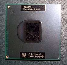
LV (ULV), "Sossaman"
 | |
| Produced | From 2006 to 2008 |
|---|---|
| Max. CPU clock rate | 1667 MHz to 2167 MHz |
| FSB speeds | 667 MT/s |
| Min. feature size | 65 nm |
| Instruction set | x86 |
| Microarchitecture | Enhanced Pentium M |
| CPUID code | 06Ex |
| Product code | 80539 |
| Cores | 2 |
| L2 cache | 2 MB |
| Application | DP Server |
| Package(s) | |
| Brand name(s) |
|
On 14 March 2006, Intel released a dual-core processor codenamed Sossaman and branded as Xeon LV (low-voltage). Subsequently an ULV (ultra-low-voltage) version was released. The Sossaman was a low-/ultra-low-power and double-processor capable CPU (like AMD Quad FX), based on the "Yonah" processor, for ultradense non-consumer environment (i.e., targeted at the blade-server and embedded markets), and was rated at a thermal design power (TDP) of 31 W (LV: 1.66 GHz, 2 GHz and 2.16 GHz) and 15 W (ULV: 1.66 GHz).[6] As such, it supported most of the same features as earlier Xeons: Virtualization Technology, 667 MT/s front side bus, and dual-core processing, but did not support 64-bit operations, so it could not run 64-bit server software, such as Microsoft Exchange Server 2007, and therefore was limited to 16 GB of memory. A planned successor, codenamed "Merom MP" was to be a drop-in upgrade to enable Sossaman-based servers to upgrade to 64-bit capability. However, this was abandoned in favour of low-voltage versions of the Woodcrest LV processor leaving the Sossaman at a dead-end with no upgrade path.
| Model | Speed (GHz) | L2 Cache (MB) | FSB (MHz) | TDP (W) |
|---|---|---|---|---|
| ULV 1.66 | 1.66 | 2 | 667 | 15 |
| LV 1.66 | 1.66 | 2 | 667 | 31 |
| LV 2.00 | 2.00 | 2 | 667 | 31 |
| LV 2.16 | 2.16 | 2 | 667 | 31 |
Core-based Xeon
Dual-Core
3000-series "Conroe"
The 3000 series, codenamed Conroe (product code 80557) dual-core Xeon (branded) CPU,[7] released at the end of September 2006, was the first Xeon for single-CPU operation. The same processor is branded as Core 2 Duo or as Pentium Dual-Core and Celeron, with varying features disabled. They use LGA 775 (Socket T), operate on a 1066 MHz front-side bus, support Enhanced Intel Speedstep Technology and Intel Virtualization Technology but do not support Hyper-Threading. Conroe Processors with a number ending in "5" have a 1333 MT/s FSB.[8]
| Model | Speed (GHz) | L2 Cache (MB) | FSB (MHz) | TDP (W) |
|---|---|---|---|---|
| 3040 | 1.86 | 2 | 1066 | 65 |
| 3050 | 2.13 | 2 | 1066 | 65 |
| 3055* | 2.13 | 4 | 1066 | 65 |
| 3060 | 2.4 | 4 | 1066 | 65 |
| 3065 | 2.33 | 4 | 1333 | 65 |
| 3070 | 2.66 | 4 | 1066 | 65 |
| 3075 | 2.66 | 4 | 1333 | 65 |
| 3080* | 2.93 | 4 | 1066 | 65 |
| 3085 | 3.00 | 4 | 1333 | 65 |
- Models marked with a star are not present in Intel's database[9]
3100-series "Wolfdale"
The 3100 series, codenamed Wolfdale (product code 80570) dual-core Xeon (branded) CPU, was just a rebranded version of the Intel's mainstream Core 2 Duo E7000/E8000 and Pentium Dual-Core E5000 processors, featuring the same 45 nm process and 6 MB of L2 cache. Unlike most Xeon processors, they only support single-CPU operation. They use LGA 775 (Socket T), operate on a 1333 MHz front-side bus, support Enhanced Intel Speedstep Technology and Intel Virtualization Technology but do not support Hyper-Threading.
| Model | Speed (GHz) | L2 Cache (MB) | FSB (MHz) | TDP (W) |
|---|---|---|---|---|
| E3110 | 3.00 | 6 | 1333 | 65 |
| L3110 | 3.00 | 6 | 1333 | 45 |
| E3120 | 3.16 | 6 | 1333 | 65 |
5100-series "Woodcrest"
 | |
| Produced | From 2006 to 2009 |
|---|---|
| Max. CPU clock rate | 1.6 GHz to 3.0 GHz |
| FSB speeds | 1066 MT/s to 1333 MT/s |
| Min. feature size | 65nm |
| Instruction set | x86 |
| Microarchitecture | Core |
| CPUID code | 06Fx |
| Product code | 80556 |
| Cores | 2 |
| L2 cache | 4 MB |
| Application | DP Server |
| Package(s) | |
| Brand name(s) |
|
On 26 June 2006, Intel released the dual-core CPU (Xeon branded 5100 series) codenamed Woodcrest (product code 80556); it was the first Intel Core microarchitecture processor to be launched on the market. It is a server and workstation version of the Intel Core 2 processor. Intel claims that it provides an 80% boost in performance, while reducing power consumption by 20% relative to the Pentium D.
Most models have a 1333 MT/s FSB, except for the 5110 and 5120, which have a 1066 MT/s FSB. The fastest processor (5160) operates at 3.0 GHz. All Woodcrests use LGA 771 and all except two models have a TDP of 65 W. The 5160 has a TDP of 80 W and the 5148LV (2.33 GHz) has a TDP of 40 W. The previous generation Xeons had a TDP of 130 W. All models support Intel 64 (Intel's x86-64 implementation), the XD bit, and Virtualization Technology, with the "Demand Based Switching" power management option only on Dual-Core Xeon 5140 or above. Woodcrest has 4 MB of shared L2 Cache.
| Model | Speed (GHz) | L2 Cache (MB) | FSB (MHz) | TDP (W) |
|---|---|---|---|---|
| 5110 | 1.60 | 4 | 1066 | 65 |
| 5120 | 1.83 | 4 | 1066 | 65 |
| 5128 | 1.83 | 4 | 1066 | 40 |
| 5130 | 2.0 | 4 | 1333 | 65 |
| 5138 | 2.13 | 4 | 1066 | 35 |
| 5140 | 2.33 | 4 | 1333 | 65 |
| 5148 | 2.33 | 4 | 1333 | 40 |
| 5150 | 2.66 | 4 | 1333 | 65 |
| 5160 | 3.00 | 4 | 1333 | 80 |
5200-series "Wolfdale-DP"
| Produced | From 2007 to present |
|---|---|
| Max. CPU clock rate | 1866 MHz to 3500 MHz |
| FSB speeds | 1066 MT/s to 1600 MT/s |
| Min. feature size | 45 nm |
| Instruction set | x86 |
| Microarchitecture | Penryn |
| CPUID code | 1067x |
| Product code | 80573 |
| Cores | 2 |
| L2 cache | 6 MB |
| Application | DP Server |
| Package(s) | |
| Brand name(s) |
|
On 11 November 2007, Intel released the dual-core CPU (Xeon branded 5200 series) codenamed Wolfdale-DP (product code 80573).[10] It is built on a 45 nm process like the desktop Core 2 Duo and Xeon-SP Wolfdale, featuring Intel 64 (Intel's x86-64 implementation), the XD bit, and Virtualization Technology. It is unclear whether the "Demand Based Switching" power management is available on the L5238.[11] Wolfdale has 6 MB of shared L2 Cache.
| Model | Speed (GHz) | L2 Cache (MB) | FSB (MHz) | TDP (W) |
|---|---|---|---|---|
| E5205 | 1.86 | 6 | 1066 | 65 |
| L5238 | 2.66 | 6 | 1333 | 35 |
| L5240 | 3.00 | 6 | 1333 | 40 |
| X5260 | 3.33 | 6 | 1333 | 80 |
| X5270 | 3.50 | 6 | 1333 | 80 |
| X5272 | 3.40 | 6 | 1600 | 80 |
7200-series "Tigerton"
The 7200 series, codenamed Tigerton (product code 80564) is an MP-capable processor, similar to the 7300 series, but, in contrast, only one core is active on each silicon chip and the other one is disabled, resulting in a dual-core processor.[12][13][14][15]
| Model | Speed (GHz) | L2 Cache (MB) | FSB (MHz) | TDP (W) |
|---|---|---|---|---|
| E7210 | 2.40 | 2 × 4 | 1066 | 80 |
| E7220 | 2.93 | 2 × 4 | 1066 | 80 |
Quad-Core and Multi-Core Xeon
3200-series "Kentsfield"
Intel released relabeled versions of its quad-core (2×2) Core 2 Quad processor as the Xeon 3200-series (product code 80562) on 7 January 2007.[16] The 2 × 2 "quad-core" (dual-die dual-core[17]) comprised two separate dual-core die next to each other in one CPU package. The models are the X3210, X3220 and X3230, running at 2.13 GHz, 2.4 GHz and 2.66 GHz, respectively.[18] Like the 3000-series, these models only support single-CPU operation and operate on a 1066 MHz front-side bus. It is targeted at the "blade" market. The X3220 is also branded and sold as Core2 Quad Q6600, the X3230 as Q6700.
| Model | Speed (GHz) | L2 Cache (MB) | FSB (MHz) | TDP (W) |
|---|---|---|---|---|
| X3210 | 2.13 | 2 × 4 | 1066 | 100/105 |
| X3220 | 2.40 | 2 × 4 | 1066 | 100/105 |
| X3230 | 2.66 | 2 × 4 | 1066 | 100 |
3300-series "Yorkfield"
Intel released relabeled versions of its quad-core Core 2 Quad Yorkfield Q9400 and Q9x50 processors as the Xeon 3300-series (product code 80569). This processor comprises two separate dual-core dies next to each other in one CPU package and manufactured in a 45 nm process. The models are the X3320, X3350, X3360, X3370 and X3380, running at 2.50 GHz, 2.66 GHz, 2.83 GHz, 3.0 GHz, and 3.16 GHz, respectively. The L2 cache is a unified 6 MB per die (except for the X3320 with a smaller 3 MB L2 cache per die), and a front-side bus of 1333 MHz. All models feature Intel 64 (Intel's x86-64 implementation), the XD bit, and Virtualization Technology, as well as "Demand Based Switching".
The Yorkfield-CL (product code 80584) variant of these processors are X3323, X3353 and X3363. They have a reduced TDP of 80W and are made for single-CPU LGA 771 systems instead of LGA 775, which is used in all other Yorkfield processors. In all other respects, they are identical to their Yorkfield counterparts.
5300-series "Clovertown"
 | |
| Produced | From 2006 to present |
|---|---|
| Max. CPU clock rate | 1600 MHz to 3000 MHz |
| FSB speeds | 1066 MT/s to 1333 |
| Min. feature size | 65 nm |
| Instruction set | x86 |
| Microarchitecture | Core |
| CPUID code | 06Fx |
| Product code | 80574 |
| Cores | 4 |
| L2 cache | 2×4 MB |
| Application | DP Server |
| Package(s) | |
| Brand name(s) |
|
A quad-core (2×2) successor of the Woodcrest for DP segment, consisting of two dual-core Woodcrest chips in one package similarly to the dual-core Pentium D branded CPUs (two single-core chips) or the quad-core Kentsfield. All Clovertowns use the LGA 771 package. The Clovertown has been usually implemented with two Woodcrest dies on a multi-chip module, with 8 MB of L2 cache (4 MB per die). Like Woodcrest, lower models use a 1066 MT/s FSB, and higher models use a 1333 MT/s FSB. Intel released Clovertown, product code 80563, on 14 November 2006[19] with models E5310, E5320, E5335, E5345, and X5355, ranging from 1.6 GHz to 2.66 GHz. All models support: MMX, SSE, SSE2, SSE3, SSSE3, Intel 64, XD bit (an NX bit implementation), Intel VT. The E and X designations are borrowed from Intel's Core 2 model numbering scheme; an ending of −0 implies a 1066 MT/s FSB, and an ending of −5 implies a 1333 MT/s FSB.[18] All models have a TDP of 80 W with the exception of the X5355, which has a TDP of 120 W, and the X5365, which has a TDP of 150 W. A low-voltage version of Clovertown with a TDP of 50 W has a model numbers L5310, L5320 and L5335 (1.6 GHz, 1.86 GHz and 2.0 GHz respectively). The 3.0 GHz X5365 arrived in July 2007, and became available in the Apple Mac Pro[20] on 4 April 2007.[21][22] The X5365 performs up to around 38 GFLOPS in the LINPACK benchmark.[23]
| Model | Speed (GHz) | L2 Cache (MB) | FSB (MHz) | TDP (W) |
|---|---|---|---|---|
| E5310 | 1.60 | 2 × 4 | 1066 | 80 |
| L5310 | 1.60 | 2 × 4 | 1066 | 50 |
| E5320 | 1.86 | 2 × 4 | 1066 | 80 |
| L5320 | 1.86 | 2 × 4 | 1066 | 50 |
| E5335 | 2.00 | 2 × 4 | 1333 | 80 |
| L5335 | 2.00 | 2 × 4 | 1333 | 50 |
| E5345 | 2.33 | 2 × 4 | 1333 | 80 |
| X5355 | 2.66 | 2 × 4 | 1333 | 120 |
| X5365 | 3.00 | 2 × 4 | 1333 | 150 |
5400-series "Harpertown"
| Produced | From 2007 to present |
|---|---|
| Max. CPU clock rate | 2000 MHz to 3400 MHz |
| FSB speeds | 1066 MT/s to 1600 |
| Min. feature size | 45 nm |
| Instruction set | x86 |
| Microarchitecture | Penryn |
| CPUID code | 1067x |
| Product code | 80574 |
| Cores | 4 |
| L2 cache | 2 × 6 MB |
| Application | DP Server |
| Package(s) | |
| Brand name(s) |
|
On 11 November 2007 Intel presented Yorkfield-based Xeons – called Harpertown (product code 80574) – to the public. This family consists of dual die quad-core CPUs manufactured on a 45 nm process and featuring 1066 MHz, 1333 MHz, 1600 MHz front-side buses, with TDP rated from 40 W to 150 W depending on the model. These processors fit in the LGA 771 package. All models feature Intel 64 (Intel's x86-64 implementation), the XD bit, and Virtualization Technology. All except the E5405 and L5408 also feature Demand Based Switching.[24][25] The supplementary character in front of the model-number represents the thermal rating: an L depicts a TDP of 40 W or 50 W, an E depicts 80 W whereas an X is 120 W TDP or above. The speed of 3.00 GHz comes as four models, two models with 80 W TDP two other models with 120 W TDP with 1333 MHz or 1600 MHz front-side bus respectively. The fastest Harpertown is the X5492 whose TDP of 150 W is higher than those of the Prescott-based Xeon DP but having twice as many cores. (The X5482 is also sold under the name "Core 2 Extreme QX9775" for use in the Intel SkullTrail system.)
Intel 1600 MHz front-side bus Xeon processors will drop into the Intel 5400 (Seaburg) chipset whereas several mainboards featuring the Intel 5000/5200-chipset are enabled to run the processors with a 1333 MHz front-side bus speed. Seaburg features support for dual PCIe 2.0 x16 slots and up to 128 GB of memory.[26][27]
| Model | Speed (GHz) | L2 Cache (MB) | FSB (MHz) | TDP (W) |
|---|---|---|---|---|
| E5405 | 2.00 | 2 × 6 | 1333 | 80 |
| L5408 | 2.13 | 2 × 6 | 1066 | 40 |
| E5410 | 2.33 | 2 × 6 | 1333 | 80 |
| L5410 | 2.33 | 2 × 6 | 1333 | 50 |
| E5420 | 2.50 | 2 × 6 | 1333 | 80 |
| L5420 | 2.50 | 2 × 6 | 1333 | 50 |
| E5430 | 2.66 | 2 × 6 | 1333 | 80 |
| L5430 | 2.66 | 2 × 6 | 1333 | 50 |
| E5440 | 2.83 | 2 × 6 | 1333 | 80 |
| X5450 | 3.00 | 2 × 6 | 1333 | 120 |
| E5450 | 3.00 | 2 × 6 | 1333 | 80 |
| X5460 | 3.16 | 2 × 6 | 1333 | 120 |
| X5470 | 3.33 | 2 × 6 | 1333 | 120 |
| E5462 | 2.80 | 2 × 6 | 1600 | 80 |
| E5472 | 3.00 | 2 × 6 | 1600 | 80 |
| X5472 | 3.00 | 2 × 6 | 1600 | 120 |
| X5482 | 3.20 | 2 × 6 | 1600 | 150 |
| X5492 | 3.40 | 2 × 6 | 1600 | 150 |
7300-series "Tigerton"
| Produced | From 2007 to present |
|---|---|
| Max. CPU clock rate | 1600 MHz to 2933 MHz |
| FSB speeds | 1066 MT/s |
| Min. feature size | 65 nm |
| Instruction set | x86 |
| Microarchitecture | Core |
| CPUID code | 06Fx |
| Product code |
80564 80565 |
| Cores | 4 |
| L2 cache | 2×2 or 2×4 MB |
| Application | MP Server |
| Package(s) | |
| Brand name(s) |
|
The 7300 series, codenamed Tigerton (product code 80565) is a four-socket (packaged in Socket 604) and more capable quad-core processor, consisting of two dual core Core2 architecture silicon chips on a single ceramic module, similar to Intel's Xeon 5300 series Clovertown processor modules.[28]
The 7300 series uses Intel's Caneland (Clarksboro) platform.
Intel claims the 7300 series Xeons offer more than twice the performance per watt as Intel's previous generation 7100 series. The 7300 series' Caneland chipset provides a point to point interface allowing the full front side bus bandwidth per processor.
The 7xxx series is aimed at the large server market, supporting configurations of up to 32 CPUs per host.
| Model | Speed (GHz) | L2 Cache (MB) | FSB (MHz) | TDP (W) |
|---|---|---|---|---|
| E7310 | 1.60 | 2×2 | 1066 | 80 |
| E7320 | 2.13 | 2×2 | 1066 | 80 |
| E7330 | 2.40 | 2×3 | 1066 | 80 |
| E7340 | 2.40 | 2×4 | 1066 | 80 |
| L7345 | 1.86 | 2×4 | 1066 | 50 |
| X7350 | 2.93 | 2×4 | 1066 | 130 |
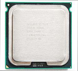
7400-series "Dunnington"
|
Exposed die of an Intel Xeon E7440 (heat spreader removed) | |
| Produced | From 2008 to present |
|---|---|
| Max. CPU clock rate | 2133 MHz |
| FSB speeds | 1066 MT/s |
| Min. feature size | 45 nm |
| Instruction set | x86 |
| Microarchitecture | Penryn |
| CPUID code | 106D1 |
| Product code | 80582 |
| Cores | 6 |
| L1 cache | 6 × 96 KB |
| L2 cache | 3 × 3 MB |
| L3 cache | 16 MB |
| Application | MP Server |
| Package(s) | |
| Brand name(s) |
|

Dunnington[29] – the last CPU of the Penryn generation and Intel's first multi-core (above two) die – features a single-die six- (or hexa-) core design with three unified 3 MB L2 caches (resembling three merged 45 nm dual-core Wolfdale dies), and 96 kB L1 cache (Data) and 16 MB of L3 cache. It features 1066 MHz FSB, fits into the Tigerton's mPGA604 socket, and is compatible with both the Intel Caneland and IBM X4 chipsets. These processors support DDR2-1066 (533 MHz), and have a maximum TDP below 130 W. They are intended for blades and other stacked computer systems. Availability was scheduled for the second half of 2008. It was followed shortly by the Nehalem microarchitecture. Total transistor count is 1.9 billion.[30]
Announced on 15 September 2008.[31]
| Model | Speed (GHz) | L3 Cache (MB) | FSB (MHz) | TDP (W) | Cores |
|---|---|---|---|---|---|
| E7420 | 2.13 | 8 | 1066 | 90 | 4 |
| E7430 | 2.13 | 12 | 1066 | 90 | 4 |
| E7440 | 2.40 | 16 | 1066 | 90 | 4 |
| L7445 | 2.13 | 12 | 1066 | 50 | 4 |
| E7450 | 2.40 | 12 | 1066 | 90 | 6 |
| L7455 | 2.13 | 12 | 1066 | 65 | 6 |
| X7460 | 2.66 | 16 | 1066 | 130 | 6 |
Nehalem-based Xeon
3400-series "Lynnfield"
Xeon 3400-series processors based on Lynnfield fill the gap between the previous 3300-series "Yorkfield" processors and the newer 3500-series "Bloomfield". Like Bloomfield, they are quad-core single-package processors based on the Nehalem microarchitecture, but were introduced almost a year later, in September 2009. The same processors are marketed for mid-range to high-end desktops systems as Core i5 and Core i7. They have two integrated memory channels as well as PCI Express and Direct Media Interface (DMI) links, but no QuickPath Interconnect (QPI) interface.
3400-series "Clarkdale"
At low end of the 3400-series is not a Lynnfield but a Clarkdale processor, which is also used in the Core i3-500 and Core i5-600 processors as well as the Celeron G1000 and G6000 Pentium series. A single model was released in March 2010, the Xeon L3406. Compared to all other Clarkdale-based products, this one does not support integrated graphics, but has a much lower thermal design power of just 30 W. Compared to the Lynnfield-based Xeon 3400 models, it only offers two cores.
3500-series "Bloomfield"
Bloomfield is the codename for the successor to the Xeon Core microarchitecture, is based on the Nehalem microarchitecture and uses the same 45 nm manufacturing methods as Intel's Penryn. The first processor released with the Nehalem architecture is the desktop Intel Core i7, which was released in November 2008. This is the server version for single CPU systems. This is a single-socket Intel Xeon processor. The performance improvements over previous Xeon processors are based mainly on:
- Integrated memory controller supporting three memory channels of DDR3 UDIMM (Unbuffered) or RDIMM (Registered)
- A new point-to-point processor interconnect QuickPath, replacing the legacy front side bus
- Simultaneous multithreading by multiple cores and hyper-threading (2× per core).
| Model | Speed (GHz) | L3 Cache (MB) | QPI speed (GT/s) | DDR3 Clock (MHz) | TDP (W) | Cores | Threads | Turbo-Boost |
|---|---|---|---|---|---|---|---|---|
| W3503 | 2.40 | 4 | 4.8 | 1066 | 130 | 2 | 2 | No |
| W3505 | 2.53 | 4 | 4.8 | 1066 | 130 | 2 | 2 | No |
| W3520 | 2.66 | 8 | 4.8 | 1066 | 130 | 4 | 8 | Yes |
| W3530 | 2.80 | 8 | 4.8 | 1066 | 130 | 4 | 8 | Yes |
| W3540 | 2.93 | 8 | 4.8 | 1066 | 130 | 4 | 8 | Yes |
| W3550 | 3.06 | 8 | 4.8 | 1066 | 130 | 4 | 8 | Yes |
| W3565 | 3.20 | 8 | 4.8 | 1066 | 130 | 4 | 8 | Yes |
| W3570 | 3.2 | 8 | 6.4 | 1333 | 130 | 4 | 8 | Yes |
| W3580 | 3.33 | 8 | 6.4 | 1333 | 130 | 4 | 8 | Yes |
<span id="5500-series "Gainestown"">5500-series "Gainestown"
| Produced | From 2008 to present |
|---|---|
| Max. CPU clock rate | 1866 MHz to 3333 MHz |
| Min. feature size | 45 nm |
| Instruction set | x86 |
| Microarchitecture | Nehalem |
| CPUID code | 106Ax |
| Product code | 80602 |
| Cores | 4 |
| L2 cache | 4×256 kB |
| L3 cache | 8 MB |
| Application | DP Server |
| Package(s) | |
| Brand name(s) |
|
Gainestown or Nehalem-EP, the successor to the Xeon Core microarchitecture, is based on the Nehalem microarchitecture and uses the same 45 nm manufacturing methods as Intel's Penryn. The first processor released with the Nehalem microarchitecture is the desktop Intel Core i7, which was released in November 2008. Server processors of the Xeon 55xx range were first supplied to testers in December 2008.[32]
The performance improvements over previous Xeon processors are based mainly on:
- Integrated memory controller supporting three memory channels of DDR3 SDRAM.
- A new point-to-point processor interconnect QuickPath, replacing the legacy front side bus. Gainestown has two QuickPath interfaces.
- Hyper-threading (2× per core, starting from 5518), that was already present in pre-Core Duo processors.
| Model | Speed (GHz) | L3 Cache (MB) | QPI speed (GT/s) | DDR3 Clock (MHz) | TDP (W) | Cores | Threads | Turbo-Boost |
|---|---|---|---|---|---|---|---|---|
| E5502 | 1.87 | 4 | 4.8 | 800 | 80 | 2 | 2 | No |
| E5503 | 2.00 | 4 | 4.8 | 800 | 80 | 2 | 2 | No |
| E5504 | 2.00 | 4 | 4.8 | 800 | 80 | 4 | 4 | No |
| E5506 | 2.13 | 4 | 4.8 | 800 | 80 | 4 | 4 | No |
| L5506 | 2.13 | 4 | 4.8 | 800 | 60 | 4 | 4 | No |
| E5507 | 2.26 | 4 | 4.8 | 800 | 80 | 4 | 4 | No |
| L5518 | 2.13 | 8 | 5.86 | 1066 | 60 | 4 | 8 | Yes |
| E5520 | 2.26 | 8 | 5.86 | 1066 | 80 | 4 | 8 | Yes |
| L5520 | 2.26 | 8 | 5.86 | 1066 | 60 | 4 | 8 | Yes |
| E5530 | 2.40 | 8 | 5.86 | 1066 | 80 | 4 | 8 | Yes |
| L5530 | 2.40 | 8 | 5.86 | 1066 | 60 | 4 | 8 | Yes |
| E5540 | 2.53 | 8 | 5.86 | 1066 | 80 | 4 | 8 | Yes |
| X5550 | 2.66 | 8 | 6.4 | 1333 | 95 | 4 | 8 | Yes |
| X5560 | 2.80 | 8 | 6.4 | 1333 | 95 | 4 | 8 | Yes |
| X5570 | 2.93 | 8 | 6.4 | 1333 | 95 | 4 | 8 | Yes |
| W5580 | 3.20 | 8 | 6.4 | 1333 | 130 | 4 | 8 | Yes |
| W5590 | 3.33 | 8 | 6.4 | 1333 | 130 | 4 | 8 | Yes |
<span id="C3500/C5500-Series "Jasper Forest"">C3500/C5500-series "Jasper Forest"
| Produced | From 2010 to present |
|---|---|
| Max. CPU clock rate | 1733 MHz to 2400 MHz |
| Min. feature size | 45 nm |
| Instruction set | x86 |
| Microarchitecture | Nehalem |
| CPUID code | 106Ex |
| Product code | 80612 |
| Cores | 4 |
| L2 cache | 4×256 kB |
| L3 cache | 8 MB |
| Application | UP/DP Server |
| Package(s) | |
| Brand name(s) |
|
Jasper Forest is a Nehalem-based embedded processor with PCI Express connections on-die, core counts from 1 to 4 cores and power envelopes from 23 to 85 watts.[33]
The uni-processor version without QPI comes as LC35xx and EC35xx, while the dual-processor version is sold as LC55xx and EC55xx and uses QPI for communication between the processors. Both versions use a DMI link to communicate with the 3420 that is also used in the 3400-series Lynfield Xeon processors, but use an LGA 1366 package that is otherwise used for processors with QPI but no DMI or PCI Express links. The CPUID code of both Lynnfield and Jasper forest is 106Ex, i.e., family 6, model 30.
The Celeron P1053 belongs into the same family as the LC35xx series, but lacks some RAS features that are present in the Xeon version.
3600/5600-series "Gulftown" & "Westmere-EP"
Gulftown or Westmere-EP, a six-core 32 nm Westmere-based processor, is the basis for the Xeon 36xx and 56xx series and the Core i7-980X. It launched in the first quarter of 2010. The 36xx-series follows the 35xx-series Bloomfield uni-processor model while the 56xx-series follows the 55xx-series Gainestown dual-processor model and both are socket compatible to their predecessors.
| Model | Speed (GHz) | L3 Cache (MB) | QPI speed (GT/s) | DDR3 Clock (MHz) | TDP (W) | Cores | Threads | Turbo-Boost |
|---|---|---|---|---|---|---|---|---|
| W3670 | 3.20 | 12 | 4.8 | 1066 | 130 | 6 | 12 | Y |
| W3680 | 3.33 | 12 | 6.4 | 1333 | 130 | 6 | 12 | Y |
| W3690 | 3.46 | 12 | 6.4 | 1333 | 130 | 6 | 12 | Y |
| E5603 | 1.60 | 4 | 4.8 | 800 | 80 | 4 | 4 | N |
| E5606 | 2.13 | 8 | 4.8 | 1066 | 80 | 4 | 4 | N |
| E5607 | 2.26 | 8 | 4.8 | 1066 | 80 | 4 | 4 | N |
| L5609 | 1.86 | 12 | 4.8 | 1066 | 40 | 4 | 4 | N |
| L5618 | 1.86 | 12 | 5.86 | 1066 | 40 | 4 | 8 | Y |
| E5620 | 2.40 | 12 | 5.86 | 1066 | 80 | 4 | 8 | Y |
| L5630 | 2.13 | 12 | 5.86 | 1066 | 40 | 4 | 8 | Y |
| E5630 | 2.53 | 12 | 5.86 | 1066 | 80 | 4 | 8 | Y |
| L5638 | 2.00 | 12 | 5.86 | 1333 | 60 | 6 | 12 | Y |
| L5639 | 2.13 | 12 | 5.86 | 1333 | 60 | 6 | 12 | Y |
| L5640 | 2.26 | 12 | 5.86 | 1333 | 60 | 6 | 12 | Y |
| E5640 | 2.66 | 12 | 5.86 | 1066 | 80 | 4 | 8 | Y |
| L5645 | 2.40 | 12 | 5.86 | 1333 | 60 | 6 | 12 | Y |
| E5645 | 2.40 | 12 | 5.86 | 1333 | 80 | 6 | 12 | Y |
| E5649 | 2.53 | 12 | 5.86 | 1333 | 80 | 6 | 12 | Y |
| X5650 | 2.66 | 12 | 6.4 | 1333 | 95 | 6 | 12 | Y |
| X5660 | 2.80 | 12 | 6.4 | 1333 | 95 | 6 | 12 | Y |
| X5667 | 3.06 | 12 | 6.4 | 1333 | 95 | 4 | 8 | Y |
| X5670 | 2.93 | 12 | 6.4 | 1333 | 95 | 6 | 12 | Y |
| X5672 | 3.20 | 12 | 6.4 | 1333 | 95 | 4 | 8 | Y |
| X5675 | 3.06 | 12 | 6.4 | 1333 | 95 | 6 | 12 | Y |
| X5677 | 3.46 | 12 | 6.4 | 1333 | 130 | 4 | 8 | Y |
| X5679 | 3.20 | 12 | 6.4 | 1066 | 115 | 6 | 12 | Y |
| X5680 | 3.33 | 12 | 6.4 | 1333 | 130 | 6 | 12 | Y |
| X5687 | 3.60 | 12 | 6.4 | 1333 | 130 | 4 | 8 | Y |
| X5690 | 3.46 | 12 | 6.4 | 1333 | 130 | 6 | 12 | Y |
| X5698 | 4.40 | 12 | 6.4 | 1066 | 130 | 2 | 4 | Y |
6500/7500-series "Beckton"
 Xeon Beckton (with and without the heat spreader) | |
| Produced | From 2010 to present |
|---|---|
| Max. CPU clock rate | 1733 MHz to 2667 MHz |
| Min. feature size | 45 nm |
| Instruction set | x86 |
| Microarchitecture | Nehalem |
| CPUID code | 206Ex |
| Product code | 80604 |
| Cores | 8 |
| L2 cache | 8 × 256 kB |
| L3 cache | 24 MB |
| Application | DP/MP Server |
| Package(s) | |
| Brand name(s) |
|
Beckton or Nehalem-EX (EXpandable server market) is a Nehalem-based processor with up to eight cores and uses buffering inside the chipset to support up to 16 standard DDR3 DIMMS per CPU socket without requiring the use of FB-DIMMS.[34] Unlike all previous Xeon MP processors, Nehalem-EX uses the new LGA 1567 package, replacing the Socket 604 used in the previous models, up to Xeon 7400 "Dunnington". The 75xx models have four QuickPath interfaces, so it can be used in up-to eight-socket configurations, while the 65xx models are only for up to two sockets. Designed by the Digital Enterprise Group (DEG) Santa Clara and Hudson Design Teams, Beckton is manufactured on the P1266 (45 nm) technology. Its launch in March 2010 coincided with that of its direct competitor, AMD's Opteron 6xxx "Magny-Cours".[35]
Most models limit the number of cores and QPI links as well as the L3 Cache size in order to get a broader range of products out of the single chip design.
| Model | Speed (GHz) | L3 Cache (MB) | QPI speed (GT/s) | DDR3 Clock (MHz) | TDP (W) | Cores | Threads | Turbo-Boost |
|---|---|---|---|---|---|---|---|---|
| E6510 | 1.73 | 12 | 2×4.8 | 800 | 105 | 4 | 8 | |
| E6540 | 2.00 | 18 | 2×6.4 | 1066 | 105 | 6 | 12 | |
| X6550 | 2.00 | 18 | 2×6.4 | 1066 | 130 | 8 | 16 | |
| E7520 | 1.86 | 18 | 3×4.8 | 800 | 95 | 4 | 8 | |
| E7530 | 1.86 | 12 | 3×5.8 | 1066 | 105 | 6 | 12 | |
| E7540 | 2.00 | 18 | 4×6.4 | 1066 | 105 | 6 | 12 | |
| X7542 | 2.66 | 18 | 4×5.8 | 1066 | 130 | 6 | 6 | 0/1/1/1 |
| L7545 | 1.86 | 18 | 4×5.8 | 1066 | 95 | 6 | 12 | 0/1/3/5 |
| X7550 | 2.00 | 18 | 4×6.4 | 1066 | 130 | 8 | 16 | |
| L7555 | 1.86 | 24 | 4×5.8 | 1066 | 95 | 8 | 16 | 1/2/4/5 |
| X7560 | 2.26 | 24 | 4×6.4 | 1066 | 130 | 8 | 16 |
E7-x8xx-series "Westmere-EX"
Westmere-EX is the follow-on to Beckton/Nehalem-EX and the first Intel Chip to have ten CPU cores. The microarchitecture is the same as in the six-core Gulftown/Westmere-EP processor, but it uses the LGA 1567 package like Beckton to support up to eight sockets.
Starting with Westmere-EX, the naming scheme has changed once again, with "E7-xxxx" now signifying the high-end line of Xeon processors using a package that supports larger than two-CPU configurations, formerly the 7xxx series. Similarly, the 3xxx uniprocessor and 5xxx dual-processor series turned into E3-xxxx and E5-xxxx, respectively, for later processors.
Sandy Bridge– and Ivy Bridge–based Xeon
E3-12xx-series "Sandy Bridge"
The Xeon E3-12xx line of processors, introduced in April 2011, uses the Sandy Bridge chips that are also the base for the Core i3/i5/i7-2xxx and Celeron/Pentium Gxxx products using the same LGA 1155 socket, but with a different set of features disabled. Notably, the Xeon variants include support for ECC memory, VT-d and trusted execution that are not present on the consumer models, while only some Xeon E3 enable the integrated GPU that is present on Sandy Bridge. Like its Xeon 3400-series predecessors, the Xeon E3 only supports operation with a single CPU socket and is targeted at entry-level workstations and servers. The CPUID of this processor is 0206A7h, the product code is 80623.
E3-12xx v2-series "Ivy Bridge"
Xeon E3-12xx v2 is a minor update of the Sandy Bridge-based E3-12xx, using the 22 nm shrink, and providing slightly better performance while remaining backwards compatible. They were released in May 2012 and mirror the desktop Core i3/i5/i7-3xxx parts.
E5-14xx/24xx series "Sandy Bridge-EN" and E5-16xx/26xx/46xx-series "Sandy Bridge-EP"
The Xeon E5-16xx processors follow the previous Xeon 3500/3600-series products as the high-end single-socket platform, using the LGA 2011 package introduced with this processor. They share the Sandy Bridge-E platform with the single-socket Core i7-38xx and i7-39xx processors. The CPU chips have no integrated GPU but eight CPU cores, some of which are disabled in the entry-level products. The Xeon E5-26xx line has the same features but also enables multi-socket operation like the earlier Xeon 5000-series and Xeon 7000-series processors.
E5-14xx v2/24xx v2 series "Ivy Bridge-EN" and E5-16xx v2/26xx v2/46xx v2 series "Ivy Bridge-EP"
The Xeon E5 v2 line was an update, released in September 2013 to replace the original Xeon E5 processors with a variant based on the Ivy Bridge shrink. The maximum number of CPU cores was raised to 12 per processor module and the total L3 cache was upped to 30 MB.[36][37] The consumer version of the Xeon E5-16xx v2 processor is the Core i7-48xx and 49xx.
E7-28xx v2/48xx v2/88xx v2 series "Ivy Bridge-EX"
The Xeon E7 v2 line was an update, released in February 2014 to replace the original Xeon E7 processors with a variant based on the Ivy Bridge shrink. There was no Sandy Bridge version of these processors.
Haswell-based Xeon
E3-12xx v3 series "Haswell-WS"


Introduced in May 2013, Xeon E3-12xx v3 is the first Xeon series based on the Haswell microarchitecture. It uses the new LGA 1150 socket, which was introduced with the desktop Core i5/i7 Haswell processors, incompatible with the LGA 1155 that was used in Xeon E3 and E3 v2. As before, the main difference between the desktop and server versions is added support for ECC memory in the Xeon-branded parts. The main benefit of the new microarchitecture is better power efficiency.
E5-16xx/26xx v3 series "Haswell-EP"

Introduced in September 2014, Xeon E5-16xx v3 and Xeon E5-26xx v3 series use the new LGA 2011-v3 socket, which is incompatible with the LGA 2011 socket used by earlier Xeon E5 and E5 v2 generations based on Sandy Bridge and Ivy Bridge microarchitectures. Some of the main benefits of this generation, compared to the previous one, are improved power efficiency, higher core counts, and bigger last level caches (LLCs). Following the already used nomenclature, Xeon E5-26xx v3 series allows dual-socket operation.
One of the new features of this generation is that Xeon E5 v3 models with more than 10 cores support cluster on die (COD) operation mode, allowing CPU's multiple columns of cores and LLC slices to be logically divided into what is presented as two non-uniform memory access (NUMA) CPUs to the operating system. By keeping data and instructions local to the "partition" of CPU which is processing them, thus decreasing the LLC access latency, COD brings performance improvements to NUMA-aware operating systems and applications.[38]
E7-48xx/88xx v3 series "Haswell-EX"
Introduced in May 2015, Xeon E7-48xx v3 and Xeon E7-88xx v3 series provide higher core counts, higher per-core performance and improved reliability features, compared to the previous Xeon E7 v2 generation. Following the usual SKU nomenclature, Xeon E7-48xx v3 and E7-88xx v3 series allow multi-socket operation, supporting up to quad- and eight-socket configurations, respectively.[39][40] These processors use the LGA 2011 (R1) socket.[41]
Xeon E7-48xx v3 and E7-88xx v3 series contain a quad-channel integrated memory controller (IMC), supporting both DDR3 and DDR4 LRDIMM or RDIMM memory modules through the use of Jordan Creek (DDR3) or Jordan Creek 2 (DDR4) memory buffer chips. Both versions of the memory buffer chip connect to the processor using version 2.0 of the Intel Scalable Memory Interconnect (SMI) interface, while supporting lockstep memory layouts for improved reliability. Up to four memory buffer chips can be connected to a processor, with up to six DIMM slots supported per each memory buffer chip.[39][40]
Xeon E7-48xx v3 and E7-88xx v3 series also contain functional bug-free support for Transactional Synchronization Extensions (TSX), which was disabled via a microcode update in August 2014 for Haswell-E, Haswell-WS (E3-12xx v3) and Haswell-EP (E5-16xx/26xx v3) models, due to a bug that was discovered in the TSX implementation.[39][40][42][43][44][45]
Broadwell-based Xeon
E3-12xx v4 series "Broadwell-WS"
Introduced in June 2015, Xeon E3-12xx v4 is the first Xeon series based on the Broadwell micro architecture. It uses LGA 1150 socket, which was introduced with the desktop Core i5/i7 Haswell processors. As before, the main difference between the desktop and server versions is added support for ECC memory in the Xeon-branded parts. The main benefit of the new microarchitecture is the new lithography process, which results in better power efficiency.
Skylake-based Xeon
E3-12xx v5 series "Skylake-WS"
Introduced in Oct 2015, Xeon E3-12xx v5 is the first Xeon series based on the Skylake micro architecture. It uses new LGA 1151 socket, which was introduced with the desktop Core i5/i7 Skylake processors. As before, the main difference between the desktop and server versions is added support for ECC memory in the Xeon-branded parts.
Supercomputers
By 2013 Xeon processors were ubiquitous in supercomputers—more than 80% of the Top500 machines in 2013 used them. For the very fastest machines, much of the performance comes from compute accelerators; Intel's entry into that market was the Xeon Phi, the first machines using it appeared in the June 2012 list and by June 2013 it was used in the fastest computer in the world.
- The first Xeon-based machines in the top-10 appeared in November 2002, two clusters at Lawrence Livermore National Laboratory and at NOAA.
- The first Xeon-based machine to be in the first place of the Top500 was the Chinese Tianhe-IA in November 2010, which used a mixed Xeon-nVIDIA GPGPU configuration; it was overtaken by the Japanese K computer in 2012, but the Tianhe-2 system using 12-core Xeon E5-2692 processors and Xeon Phi cards occupied the first place in both Top500 lists of 2013.
- The SuperMUC system, using eight-core Xeon E5-2680 processors but no accelerator cards, managed fourth place in June 2012 and had dropped to tenth by November 2013
- Xeon processor-based systems are among the top 20 fastest systems by memory bandwidth as measured by the STREAM benchmark.[46]
- An Intel Xeon virtual SMP system using ScaleMP's Versatile SMP (vSMP) architecture with 128 cores and 1TB RAM.[47] This system aggregates 16 Stoakley platform (Seaburg chipset) systems with total of 32 Harpertown processors.
See also
- AMD Opteron
- Intel Xeon Phi, brand name for family of products using the Intel MIC architecture
- List of Intel Xeon microprocessors
- List of Intel microprocessors
References
- ↑ http://www.intel.com/content/www/us/en/processors/xeon/xeon-e3-1200-hd-graphics-guide.html
- ↑ Bateman, B.; et al. (February 1998). "A 450MHz 512kB Second-Level Cache with a 3.6GB/s Data Bandwidth". ISSCC Digest of Technical Papers. doi:10.1109/ISSCC.1998.672528.
- ↑ New High-End Intel Server Processors Expand Performance Leadership, Intel News Release.
- ↑
- ↑ Intel prices up Woodcrest, Tulsa server chips, The Inquirer.
- ↑ "Intel drops 32-bit dual-core LV processors". TG Daily. Retrieved 2007-07-31.
- ↑ Intel Adds Low End Xeons to Roadmap, DailyTech
- ↑ Intel Readies New Xeons and Price Cuts Archived 27 September 2007 at the Wayback Machine., WinBeta.org
- ↑ "ARK - Your Source for Intel® Product Information". Intel® ARK (Product Specs).
- ↑ HTN_WDP_Datasheet.book Archived 16 March 2008 at the Wayback Machine.
- ↑ Intel bringt neue Prozessoren für den Embedded-Markt auf Basis seiner 45nm-Fertigungstechnologie
- ↑ "Intel bares Tigerton". theregister.co.uk.
- ↑ Donald Melanson. "Intel previews quad-core Xeon "Tigerton" server processor". Engadget. AOL.
- ↑ "THE INQUIRER - News, reviews and opinion for tech buffs". theinquirer.net. Archived from the original on 19 April 2007.
- ↑ "Archived copy" (PDF). Archived from the original (PDF) on 25 October 2007. Retrieved 19 September 2007.
- ↑ Intel Hard-Launches Three New Quad-core Processors, DailyTech
- ↑ "Intel Clovertowns step up, reduce power". TG Daily. Retrieved 2007-09-05.
- 1 2 Quad-core Xeon Details Unveiled, DailyTech
- ↑ Intel Ignites Quad-Core Era, Intel News Release.
- ↑ Apple - Mac Pro - The fastest, most powerful Mac ever.
- ↑
- ↑ Intel Readies New Xeons and Price Cuts, DailyTech
- ↑ Intel® Xeon® Processor E5-2600 v4 Family World Record
- ↑ Quad-Core Intel Xeon Processor E5405, Intel ARK (Automated Relational Knowledgebase)
- ↑ Intel® Xeon® Processor L5408, Intel ARK (Automated Relational Knowledgebase)
- ↑ Intel Readies 1600 MHz Front-Side Bus Xeons, DailyTech
- ↑ Intel Xeons Coming With 1600MHz FSB, TrustedReviews
- ↑ Intel Launches First Industry-Standard Quad-Core Products for High-End, Multi-Processor Servers, Intel Corporation, 5 September 2007, retrieved 2010-06-25
- ↑ Valich, Theo (25 February 2008). "Intel six-core coming in 2008". TG Daily. Tigervision Media. Retrieved 2008-02-26.
- ↑ "Chipzilla unveils six-core 'Dunnington' Xeons". theregister.co.uk.
- ↑ "Intel® Xeon® Processor E7 Family". Intel.
- ↑ AnandTech: Intel Xeon 5570: Smashing SAP records, 16 December 2008
- ↑ "Intel demos Moorestown, embeds Nehalem". theregister.co.uk.
- ↑ "Nehalem-EX: 2.3 billion transistors, eight cores, one die".
- ↑ Intel's next bunch of fun CPUs moves to 2010 Archived 4 March 2009 at the Wayback Machine.
- ↑ Timothy Prickett Morgan (10 September 2013). "Intel carves up Xeon E5-2600 v2 chips for two-socket boxes". The Register. Retrieved 13 September 2013.
- ↑ "Intel Introduces Highly Versatile Datacenter Processor Family Architected for New Era of Services". Press release. 10 September 2013. Retrieved 13 September 2013.
- ↑ Johan De Gelas (2014-09-08). "Intel Xeon E5 Version 3, Up to 18 Haswell EP Cores: The Magic Inside the Uncore". AnandTech. Retrieved 2014-09-09.
- 1 2 3 Anthony Shvets (2015-05-07). "Intel launches Xeon E7 v3 server processors". cpu-world.com. Retrieved 2015-05-16.
- 1 2 3 Johan De Gelas (2015-05-08). "The Intel Xeon E7-8800 v3 Review: The POWER8 Killer?". AnandTech. Retrieved 2015-05-16.
- ↑ Hassan Mujtaba (2015-05-06). "Intel Unleashes Haswell-EX Xeon E7 V3 Processors – Up to 18 Cores, 45 MB L3 Cache, 12 TB DDR4 Memory Support and 5.7 Billion Transistors". wccftech.com. Retrieved 2016-01-29.
- ↑ Ian Cutress (2014-08-12). "Intel Disables TSX Instructions: Erratum Found in Haswell, Haswell-E/EP, Broadwell-Y". AnandTech. Retrieved 2014-08-30.
- ↑ "Transactional Synchronization in Haswell". Intel. 2012-02-07. Retrieved 2012-02-07.
- ↑ Wasson, Scott (2014-08-12). "Errata prompts Intel to disable TSX in Haswell, early Broadwell CPUs". The Tech Report. Retrieved 2014-08-12.
- ↑ "Desktop 4th Generation Intel Core Processor Family, Desktop Intel Pentium Processor Family, and Desktop Intel Celeron Processor Family: Specification Update (Revision 014)" (PDF). Intel. June 2014. p. 46. Retrieved 2014-08-13.
Under a complex set of internal timing conditions and system events, software using the Intel TSX (Transactional Synchronization Extensions) instructions may observe unpredictable system behavior.
- ↑ STREAM benchmark, Dr. John D. McCalpin
- ↑ "Stream Benchmark Results - Top 20 Set". virginia.edu.
External links
| Wikimedia Commons has media related to Xeon. |
- Server processors at the Intel website
- Intel look inside: Xeon E5 v3 (Grantley) launch, Intel, September 2014