Adder (electronics)
An adder, also called summer, is a digital circuit that performs addition of numbers. In many computers and other kinds of processors, adders are used not only in the arithmetic logic units, but also in other parts of the processor, where they are used to calculate addresses, table indices, increment and decrement operators, and similar operations.
Although adders can be constructed for many numerical representations, such as binary-coded decimal or excess-3, the most common adders operate on binary numbers. In cases where two's complement or ones' complement is being used to represent negative numbers, it is trivial to modify an adder into an adder–subtractor. Other signed number representations require more logic around the basic adder.
Half adder

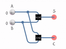
The half adder adds two single binary digits A and B. It has two outputs, sum (S) and carry (C). The carry signal represents an overflow into the next digit of a multi-digit addition. The value of the sum is 2C + S. The simplest half-adder design, pictured on the right, incorporates an XOR gate for S and an AND gate for C. With the addition of an OR gate to combine their carry outputs, two half adders can be combined to make a full adder.[1] The half adder adds two input bits and generates a carry and sum, which are the two outputs of a half adder. The input variables of a half adder are called the augend and addend bits. The output variables are the sum and carry. The truth table for the half adder is:
| Inputs | Outputs | ||
|---|---|---|---|
| A | B | C | S |
| 0 | 0 | 0 | 0 |
| 1 | 0 | 0 | 1 |
| 0 | 1 | 0 | 1 |
| 1 | 1 | 1 | 0 |
Full adder


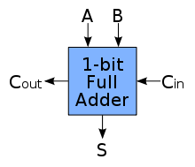
A full adder adds binary numbers and accounts for values carried in as well as out. A one-bit full adder adds three one-bit numbers, often written as A, B, and Cin; A and B are the operands, and Cin is a bit carried in from the previous less-significant stage.[2] The full adder is usually a component in a cascade of adders, which add 8, 16, 32, etc. bit binary numbers. The circuit produces a two-bit output, output carry and sum typically represented by the signals Cout and S, where .

A full adder can be implemented in many different ways such as with a custom transistor-level circuit or composed of other gates. One example implementation is with and .


In this implementation, the final OR gate before the carry-out output may be replaced by an XOR gate without altering the resulting logic. Using only two types of gates is convenient if the circuit is being implemented using simple IC chips which contain only one gate type per chip.
A full adder can be constructed from two half adders by connecting A and B to the input of one half adder, connecting the sum from that to an input to the second adder, connecting Ci to the other input and OR the two carry outputs. The critical path of a full adder runs through both XOR-gates and ends at the sum bit . Assumed that an XOR-gate takes 1 delays to complete, the delay imposed by the critical path of a full adder is equal to


The critical path of a carry runs through 1 XOR-gate in adder and through 2 gates (AND and OR) in carry-block and therefore, if AND- or OR-gates takes 1 delay to complete, has a delay of

The truth table for the full adder is:
| Inputs | Outputs | |||
|---|---|---|---|---|
| A | B | Cin | Cout | S |
| 0 | 0 | 0 | 0 | 0 |
| 0 | 0 | 1 | 0 | 1 |
| 0 | 1 | 0 | 0 | 1 |
| 1 | 0 | 0 | 0 | 1 |
| 0 | 1 | 1 | 1 | 0 |
| 1 | 0 | 1 | 1 | 0 |
| 1 | 1 | 0 | 1 | 0 |
| 1 | 1 | 1 | 1 | 1 |
More complex adders
Ripple-carry adder


It is possible to create a logical circuit using multiple full adders to add N-bit numbers. Each full adder inputs a Cin, which is the Cout of the previous adder. This kind of adder is called a ripple-carry adder, since each carry bit "ripples" to the next full adder. Note that the first (and only the first) full adder may be replaced by a half adder (under the assumption that Cin = 0).
The layout of a ripple-carry adder is simple, which allows fast design time; however, the ripple-carry adder is relatively slow, since each full adder must wait for the carry bit to be calculated from the previous full adder. The gate delay can easily be calculated by inspection of the full adder circuit. Each full adder requires three levels of logic. In a 32-bit ripple-carry adder, there are 32 full adders, so the critical path (worst case) delay is 3 × 31 (from input to later adder) + 2 (in later adder) = 95 gate delays. The general equation for the worst-case delay for a n-bit carry-ripple adder is

The delay from bit position 0 to the carry-out is a little different:
![{\displaystyle T_{{\text{CRA}}_{[0:c_{\text{out}}]}}=T_{{\text{CRA}}_{[c_{0}:c_{n}]}}(n)=n\cdot T_{c}=n\cdot 3D=3nD.}](../I/m/9aa938ea8d1eb5758793b2aa42bdd08384b765e3.svg)
The carry-in must travel through n XOR-gates in adders and n carry-generator blocks to have an effect on the carry-out.
A design with alternating carry polarities and optimized AND-OR-Invert gates can be about twice as fast.[3]
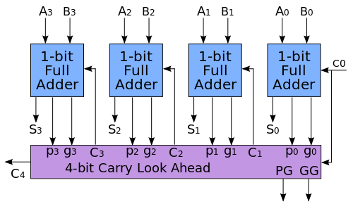
Carry-lookahead adder
To reduce the computation time, engineers devised faster ways to add two binary numbers by using carry-lookahead adders. They work by creating two signals (P and G) for each bit position, based on whether a carry is propagated through from a less significant bit position (at least one input is a 1), generated in that bit position (both inputs are 1), or killed in that bit position (both inputs are 0). In most cases, P is simply the sum output of a half adder and G is the carry output of the same adder. After P and G are generated the carries for every bit position are created. Some advanced carry-lookahead architectures are the Manchester carry chain, Brent–Kung adder, and the Kogge–Stone adder.
Some other multi-bit adder architectures break the adder into blocks. It is possible to vary the length of these blocks based on the propagation delay of the circuits to optimize computation time. These block based adders include the carry-skip (or carry-bypass) adder which will determine P and G values for each block rather than each bit, and the carry select adder which pre-generates the sum and carry values for either possible carry input (0 or 1) to the block, using multiplexers to select the appropriate result when the carry bit is known.
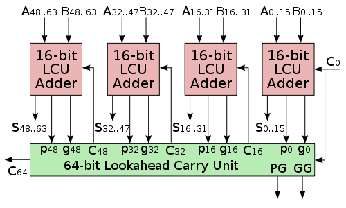
By combining multiple carry-lookahead adders, even larger adders can be created. This can be used at multiple levels to make even larger adders. For example, the following adder is a 64-bit adder that uses four 16-bit CLAs with two levels of LCUs.
Other adder designs include the carry-select adder, conditional sum adder, carry-skip adder, and carry-complete adder.
Carry-save adders
If an adding circuit is to compute the sum of three or more numbers, it can be advantageous to not propagate the carry result. Instead, three-input adders are used, generating two results: a sum and a carry. The sum and the carry may be fed into two inputs of the subsequent 3-number adder without having to wait for propagation of a carry signal. After all stages of addition, however, a conventional adder (such as the ripple-carry or the lookahead) must be used to combine the final sum and carry results.
3:2 compressors
We can view a full adder as a 3:2 lossy compressor: it sums three one-bit inputs and returns the result as a single two-bit number; that is, it maps 8 input values to 4 output values. Thus, for example, a binary input of 101 results in an output of 1 + 0 + 1 = 10 (decimal number 2). The carry-out represents bit one of the result, while the sum represents bit zero. Likewise, a half adder can be used as a 2:2 lossy compressor, compressing four possible inputs into three possible outputs.
Such compressors can be used to speed up the summation of three or more addends. If the addends are exactly three, the layout is known as the carry-save adder. If the addends are four or more, more than one layer of compressors is necessary, and there are various possible design for the circuit: the most common are Dadda and Wallace trees. This kind of circuit is most notably used in multipliers, which is why these circuits are also known as Dadda and Wallace multipliers.
References
- ↑ Geoffrey A. Lancaster (2004). Excel HSC Software Design and Development. Pascal Press. p. 180. ISBN 9781741251753.
- ↑ M. Morris Mano, Digital Logic and Computer Design, Prentice-Hall 1979, 0-13-214510-3 pp. 119–123.
- ↑ Burgess, N. (2011). Fast Ripple-Carry Adders in Standard-Cell CMOS VLSI (PDF). 20th IEEE Symposium on Computer Arithmetic. pp. 103–111.
See also
External links
- Binary adder with visual results, A tool which visually explains how to add two binary numbers submitted by user. Helpful for beginners.
- Hardware algorithms for arithmetic modules, includes description of several adder layouts with figures.
- 8-bit Full Adder and Subtractor, a demonstration of an interactive Full Adder built in JavaScript solely for learning purposes.
- Interactive Full Adder Simulation (requires Java), Interactive Full Adder circuit constructed with Teahlab's online circuit simulator.
- Interactive Half Adder Simulation (requires Java), Half Adder circuit built with Teahlab's circuit simulator.
- 4-bit Full Adder Simulation built in Verilog, and the accompanying Ripple Carry Full Adder Video Tutorial