Apple mobile application processors
Apple Inc. has developed a range of "System on Chip" (SoC) as well as "System in Package" (SiP) mobile application processors for powering their mobile consumer devices. To meet the stringent power and space constraints common to mobile devices, these chips combine a central processing unit (CPU) with other components into a single compact physical package. Johny Srouji is the executive in charge of Apple's silicon design.[1]
Early series
Prior to the introduction of the Apple "A" series of SoCs, Apple used several SoCs in early revisions of the iPhone and iPod Touch. They were specified by Apple and manufactured by Samsung. They integrate a single ARM-based processing core (CPU), a graphics processing unit (GPU), and other electronics necessary to provide mobile computing functions within a single physical package.
The APL0098 (also 8900B[2] or S5L8900) is a package on package (PoP) system on a chip (SoC) that was introduced on June 29, 2007 at the launch of the original iPhone. It includes a 412 MHz single-core ARM11 CPU and a PowerVR MBX Lite GPU. It is manufactured by Samsung on a 90 nm process.[3]
The APL0278[4] (also S5L8720) is a package on package (PoP) system on a chip (SoC) that was introduced on September 9, 2008 at the launch of the second generation iPod touch. It includes a 533 MHz single-core ARM11 CPU and a PowerVR MBX Lite GPU. It is manufactured by Samsung on a 65 nm process.[3]
The APL0298 (also S5L8920) is a package on package (PoP) system on a chip (SoC) that was introduced on June 8, 2009 at the launch of the iPhone 3GS. It includes a 600 MHz single-core Cortex-A8 CPU and a PowerVR SGX535 GPU. It is manufactured by Samsung on a 65 nm process.[5] A 45 nm die shrunk version of this SoC,[3] the APL2298 (also S5L8922), was introduced on September 9, 2009 at the launch of the third generation iPod touch.
A series
| Evolution of Apple "A" series | ||||||||||||||||||||||||||||||||||||||||||||||||||||||||||||||||||||||||||||||||||||||||||||||||||||||||||||||||||||||||||||||||||||||||||||||||||||||||||||||||||||||||||||||||||||||||||||||||||||||||||||||||||||||||||||||||
|---|---|---|---|---|---|---|---|---|---|---|---|---|---|---|---|---|---|---|---|---|---|---|---|---|---|---|---|---|---|---|---|---|---|---|---|---|---|---|---|---|---|---|---|---|---|---|---|---|---|---|---|---|---|---|---|---|---|---|---|---|---|---|---|---|---|---|---|---|---|---|---|---|---|---|---|---|---|---|---|---|---|---|---|---|---|---|---|---|---|---|---|---|---|---|---|---|---|---|---|---|---|---|---|---|---|---|---|---|---|---|---|---|---|---|---|---|---|---|---|---|---|---|---|---|---|---|---|---|---|---|---|---|---|---|---|---|---|---|---|---|---|---|---|---|---|---|---|---|---|---|---|---|---|---|---|---|---|---|---|---|---|---|---|---|---|---|---|---|---|---|---|---|---|---|---|---|---|---|---|---|---|---|---|---|---|---|---|---|---|---|---|---|---|---|---|---|---|---|---|---|---|---|---|---|---|---|---|---|---|---|---|---|---|---|---|---|---|---|---|---|---|---|---|---|
| ||||||||||||||||||||||||||||||||||||||||||||||||||||||||||||||||||||||||||||||||||||||||||||||||||||||||||||||||||||||||||||||||||||||||||||||||||||||||||||||||||||||||||||||||||||||||||||||||||||||||||||||||||||||||||||||||
| Notes:
| ||||||||||||||||||||||||||||||||||||||||||||||||||||||||||||||||||||||||||||||||||||||||||||||||||||||||||||||||||||||||||||||||||||||||||||||||||||||||||||||||||||||||||||||||||||||||||||||||||||||||||||||||||||||||||||||||
The Apple "Ax" series is a family of "Systems on Chip" (SoC) used in the iPhone, iPad, iPod Touch, and Apple TV. They integrate one or more ARM-based processing cores (CPU), a graphics processing unit (GPU), cache memory and other electronics necessary to provide mobile computing functions within a single physical package. They are designed by Apple, and manufactured by Samsung and TSMC.
Apple A4
The Apple A4 is a package on package (PoP) system on a chip (SoC) designed by Apple Inc. and manufactured by Samsung.[6] It combines an ARM Cortex-A8 CPU with a PowerVR GPU, and emphasizes power efficiency.[7] The chip commercially debuted with the release of Apple's iPad tablet;[8] followed shortly by the iPhone 4 smartphone,[9] the 4th generation iPod Touch and the 2nd generation Apple TV. It was superseded in the iPad 2, released the following year, by the Apple A5 processor.
Apple A4 is based on the ARM processor architecture.[10] The first version released ran at 1 GHz for the iPad[11] and contains an ARM Cortex-A8 CPU core paired with a PowerVR SGX 535 graphics processor (GPU)[8][12][13] built on Samsung's 45-nanometer (nm) silicon chip fabrication process.[3][14] The clock speed for the units used in the iPhone 4 and the iPod Touch (4th generation) is 800 MHz. The clock speed for the unit used in the Apple TV has not been revealed.
The Cortex-A8 core used in the A4 is thought to use performance enhancements developed by chip designer Intrinsity (which was subsequently acquired by Apple)[15] in collaboration with Samsung.[16] The resulting core, dubbed "Hummingbird", is able to run at far higher clock rates than other implementations while remaining fully compatible with the Cortex-A8 design provided by ARM.[17] Other performance improvements include additional L2 cache. The same Cortex-A8 CPU core used in the A4 is also used in Samsung's S5PC110A01 SoC.[18][19] The SGX535 in the A4 could theoretically push 35 million polygons/second and 500 million pixels/second, although real world performance may be considerably less.[20]
The A4 processor package does not contain RAM, but supports PoP installation. Hence, there is a package with two low-power 128 MB DDR SDRAM chips (totaling 256 MB) mounted on top of the A4 used in the first-generation iPad, the fourth-generation iPod Touch,[21] and the second-generation Apple TV.[22] The iPhone 4 has two 256 MB packages for a total of 512 MB.[23][24][25] The RAM is connected to the processor using ARM's 64-bit-wide AMBA 3 AXI bus. To support the iPad's demand for high graphics bandwidth, the width of the RAM data bus is double that used in previous ARM11 and ARM9 based Apple devices.[26]
Apple A5
The Apple A5 is a system on a chip (SoC) designed by Apple Inc. and manufactured by Samsung[27] that replaced the A4. The chip commercially debuted with the release of Apple's iPad 2 tablet in March 2011,[28] followed by its release in the iPhone 4S smartphone later that year. Apple claims that compared with its predecessor, the A4, the A5 CPU "can do twice the work" and the GPU has "up to nine times the graphics performance".[29]
The A5 contains a dual-core ARM Cortex-A9 CPU[30] with ARM's advanced SIMD extension, marketed as NEON, and a dual core PowerVR SGX543MP2 GPU. This GPU can push between 70 and 80 million polygons/second and has a pixel fill rate of 2 billion pixels/second. Apple lists the A5 to be clocked at 1 GHz on the iPad 2's technical specifications page,[31] though it can dynamically adjust its frequency to save battery life.[30][32] The clock speed of the unit used in the iPhone 4S is 800 MHz. Like the A4, the A5 process size is 45 nm.[33]
An updated 32 nm version of the A5 processor was used in the third generation Apple TV, the iPod Touch (5th generation), the iPad Mini, and the new version of iPad 2 (version iPad2,4).[34] The chip in the Apple TV has one core locked.[35][36] The markings of the square package indicates that it's named APL2498, and in software, the chip is called S5L8942. The 32 nm variant of the A5 provides around 15% better battery life during web browsing, 30% better when playing 3D games and approximately 20% better battery life during video playback.[37]
In March 2013, Apple released an updated version of the third generation Apple TV (AppleTV3,2) containing a smaller, single-core version of the A5 processor. Unlike the other A5 variants, this version of the A5 is not a package-on-package (PoP), having no stacked RAM. The chip is very small, just 6.1×6.2 mm, but as the decrease in size is not due to a decrease in feature size (it is still on a 32 nm fabrication process), this indicates that this A5 revision is of a new design.[38] Markings tell that it's named APL7498, and in software, the chip is called S5L8947.[39][40]
Apple A5X
The Apple A5X is a system-on-a-chip (SoC) designed by Apple Inc. that was announced on March 7, 2012 at the launch of the third generation iPad. It is a high performance variant of the Apple A5; Apple claims it has twice the graphics performance of the A5.[41] It was superseded in the fourth generation iPad by the Apple A6X processor.
This SoC has a quad-core graphics unit (PowerVR SGX543MP4) instead of the previous dual-core as well as a quad-channel memory controller that provides a memory bandwidth of 12.8 GB/sec, roughly three times more than in the A5. The added graphics cores and extra memory channels add up to a very large die size of 165 mm²,[42] for example twice the size of Nvidia Tegra 3.[43] This is mainly due to the large PowerVR SGX543MP4 GPU. The clock frequency of the dual ARM Cortex-A9 cores have been shown to operate at the same 1 GHz frequency as in A5.[44] The RAM in A5X is separate from the main CPU package.[45]
Apple A6
The Apple A6 is a package on package (PoP) system on a chip (SoC) designed by Apple that was introduced on September 12, 2012 at the launch of the iPhone 5, then a year later was inherited by its minor successor the iPhone 5C. Apple states that it is up to twice as fast and has up to twice the graphics power compared to its predecessor the Apple A5.[46] It is 22% smaller and draws less power than the 45 nm A5.[47]
The A6 is said to use a 1.3 GHz[48] custom[49] Apple-designed ARMv7 based dual-core CPU, called Swift,[50] rather than a licensed CPU from ARM like in previous designs, and an integrated 266 MHz triple-core PowerVR SGX 543MP3[51] graphics processing unit (GPU). The Swift core in the A6 uses a new tweaked instruction set, ARMv7s, featuring some elements of the ARM Cortex-A15 such as support for the Advanced SIMD v2, and VFPv4.[49] The A6 is manufactured by Samsung on a high-κ metal gate (HKMG) 32 nm process.[52]
Apple A6X
Apple A6X is a system-on-a-chip (SoC) designed by Apple Inc., introduced at the launch of the fourth generation iPad on October 23, 2012. It is a high performance variant of the Apple A6. Apple claims the A6X has twice the CPU performance and up to twice the graphics performance of its predecessor, the Apple A5X.[53]
Like the A6, this SoC continues to use the dual-core Swift CPU, but it has a new quad core GPU, quad channel memory and slightly higher 1.4 GHz CPU clock rate.[54] It uses an integrated quad-core PowerVR SGX 554MP4 graphics processing unit (GPU) running at 300 MHz and a quad-channel memory subsystem.[54][55] Compared to the A6 the A6X is 30% larger, but it continues to be manufactured by Samsung on a high-κ metal gate (HKMG) 32 nm process.[55]
Apple A7
The Apple A7 is a package on package (PoP) 64-bit system-on-a-chip (SoC) designed by Apple. Its first appearance was in the iPhone 5S, which was introduced on September 10, 2013. The chip would also be used in the iPad Air, iPad Mini 2 and iPad Mini 3. Apple states that it is up to twice as fast and has up to twice the graphics power compared to its predecessor the Apple A6.[56]
The A7 features an Apple-designed 1.3[57]–1.4[58] GHz 64-bit[59] ARMv8-A[60][61] dual-core CPU,[57] called Cyclone,[60] and an integrated PowerVR G6430 GPU in a four cluster configuration.[62] The ARMv8-A architecture doubles the number of registers of the A7 compared to the A6.[63] It now has 31 general purpose registers that are each 64-bits wide and 32 floating-point/NEON registers that are each 128-bits wide.[59] The A7 is manufactured by Samsung on a high-κ metal gate (HKMG) 28 nm process[64] and the chip includes over 1 billion transistors on a die 102 mm2 in size.[57]
Apple A8
The Apple A8 is a package on package (PoP) 64-bit system-on-a-chip (SoC) designed by Apple and manufactured by TSMC. Its first appearance was in the iPhone 6 and iPhone 6 Plus, which were introduced on September 9, 2014.[65] A year later it would drive the iPad Mini 4. Apple states that it has 25% more CPU performance and 50% more graphics performance while drawing only 50% of the power compared to its predecessor, the Apple A7.[66]
The A8 features an Apple-designed 1.4[67] GHz 64-bit[68] ARMv8-A[68] dual-core CPU, and an integrated PowerVR GX6450 GPU in a four cluster configuration.[67] The A8 is manufactured on a 20 nm process[69] by TSMC,[70] which replaced Samsung as the manufacturer of Apple's mobile device processors. It contains 2 billion transistors. Despite that being double the number of transistors compared to the A7, its physical size has been reduced by 13% to 89 mm2 (consistent with a shrink only, not known to be a new microarchitecture).[71]
Apple A8X
The Apple A8X is a 64-bit system on a chip (SoC) designed by Apple, introduced at the launch of the iPad Air 2 on October 16, 2014.[72] It is a high performance variant of the Apple A8. Apple states that it has 40% more CPU performance and 2.5 times the graphics performance of its predecessor, the Apple A7.[72][73]
Unlike the A8, this SoC uses a triple-core CPU, a new octa-core GPU, dual channel memory and slightly higher 1.5 GHz CPU clock rate.[74] It uses an integrated octa-core PowerVR GXA6850 graphics processing unit (GPU) running at 450 MHz and a dual-channel memory subsystem.[74] It's manufactured by TSMC on their 20 nm fabrication process, and consists of 3 billion transistors.
Apple A9
The Apple A9 is a 64-bit ARM based system on a chip (SoC) designed by Apple Inc. It first appeared in the iPhone 6S and 6S Plus, which were introduced on September 9, 2015.[75] Apple states that it has 70% more CPU performance and 90% more graphics performance compared to its predecessor, the Apple A8.[75] It is dual sourced, a first for an Apple SoC; it is manufactured by Samsung on their 14 nm FinFET LPE process and by TSMC on their 16 nm FinFET process. It was subsequently included in the iPhone SE.
Apple A9X
The Apple A9X is a 64-bit system on a chip (SoC) designed by Apple Inc. It first appeared in the iPad Pro, which was announced on September 9, 2015.[76] It purportedly offers double the memory bandwidth and double the storage performance of its predecessor, the Apple A8X. It's manufactured by TSMC using a 16 nm FinFET process.[77]
Apple A10 Fusion
The Apple A10 Fusion is a 64-bit ARM based system on a chip (SoC) designed by Apple Inc. It first appeared in the iPhone 7 and 7 Plus, which were introduced on September 7, 2016.[78] It has a new quad core design with two high performance cores, and two smaller highly efficient cores. It is made by TSMC on their 16 nm FinFET process.
S series
The Apple "Sx" series is a family of "Systems in Package" (SiP) used in the Apple Watch. It uses a customized application processor that together with memory, storage and support processors for wireless connectivity, sensors and I/O comprise a complete computer in a single package. They are designed by Apple, and manufactured by contract manufacturers such as Samsung.
Apple S1
The Apple S1 is an integrated computer designed by Apple and as such it includes memory, storage and support circuits like wireless modems and I/O controllers in a sealed integrated package. It was announced on September 9, 2014 as part of the "Wish we could say more" event. Its first appearance was in the Apple Watch.[79]
Apple S1P
Used in Apple Watch Series 1 with a dual-core processor.
Apple S2
Used in the Apple Watch Series 2 with a dual-core processor and a built in GPS.
W series
The Apple Wx series is a series of custom made processors with focus on wireless connectivity for headphones.
Apple W1
The Apple W1 chip is a SoC from Apple used in their wireless AirPods and a select variety of Beats headphones.[80][81] It maintains a Bluetooth[82] Class 1 connection with a computer device and decodes the audio stream that is sent to it.[83]
T series
Apple T1
The Apple T1 chip is an ARMv7 SoC from Apple driving the Touch ID sensor of the 2016 MacBook Pro.[84] The chip operates as a secure enclave for the processing and encryption of fingerprints. The T1 runs its own version of watchOS, separate from the Intel CPU running macOS.[85]
List of Apple processors
A series
| Name | Model no. | Image | Semiconductor technology | Die size | #Transistors | CPU ISA | CPU | CPU cache | GPU | Memory technology | Introduced | Utilizing devices |
|---|---|---|---|---|---|---|---|---|---|---|---|---|
| APL0098 | 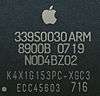 |
90 nm[5] | 72 mm2[3] | ARMv6 | 412 MHz single-core ARM11 | L1i: 16 KB L1d: 16 KB |
PowerVR MBX Lite | 16-bit Single-channel 133 MHz LPDDR (533 MB/sec)[86] | June 2007 | |||
| APL0278 |  |
65 nm[3] | 36 mm2[3] | ARMv6 | 412–533 MHz single-core ARM11 | L1i: 16 KB L1d: 16 KB |
PowerVR MBX Lite | 32-bit Single-channel 133 MHz LPDDR(1066 MB/sec) | September 2008 |
| ||
| APL0298 | 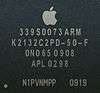 |
65 nm[5] | 71.8 mm2[14] | ARMv7 | 600 MHz single-core Cortex-A8 | L1i: 32 KB L1d: 32 KB L2: 256 KB |
PowerVR SGX535 | 32-bit Single-channel 200 MHz LPDDR (1.6 GB/sec) | June 2009 | |||
| APL2298 | 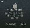 |
45 nm[3] | 41.6 mm2[3] | ARMv7 | 600–800 MHz single-core Cortex-A8 | L1i: 32 KB L1d: 32 KB L2: 256 KB |
PowerVR SGX535 | 32-bit Single-channel 200 MHz LPDDR (1.6 GB/sec) | September 2009 | |||
| A4 | APL0398 | 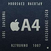 |
45 nm[3][14] | 53.3 mm2[3][14] | ARMv7 | 0.8–1.0 GHz single-core Cortex-A8 | L1i: 32 KB L1d: 32 KB L2: 512 KB |
PowerVR SGX535[88] | 32-bit Dual-channel 200 MHz LPDDR (3.2 GB/sec) | March 2010 | ||
| A5 | APL0498 | 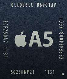 |
45 nm[33] | 122.2 mm2[33] | ARMv7 | 0.8–1.0 GHz dual-core Cortex-A9 | L1i: 32 KB L1d: 32 KB L2: 1 MB |
PowerVR SGX543MP2 (dual-core) @ 200 MHz (12.8 GFLOPS)[89] | 32-bit Dual-channel 400 MHz LPDDR2-800 (6.4 GB/sec) | March 2011 | ||
| APL2498 | 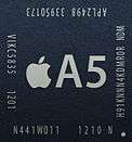 |
32 nm HKMG[34] | 69.6 mm2[34] | 0.8–1.0 GHz dual-core Cortex-A9 (one core locked in Apple TV) | L1i: 32 KB L1d: 32 KB L2: 1 MB |
PowerVR SGX543MP2 (dual-core) @ 200 MHz (12.8 GFLOPS)[89] | 32-bit Dual-channel 400 MHz LPDDR2-800 (6.4 GB/sec) | March 2012 | ||||
| APL7498 |  |
32 nm HKMG[40] | 37.8 mm2[40] | Single-core Cortex-A9 | L1i: 32 KB L1d: 32 KB L2: 1 MB |
PowerVR SGX543MP2 (dual-core) @ 200 MHz (12.8 GFLOPS)[89] | 32-bit Dual-channel 400 MHz LPDDR2-800 (6.4 GB/sec) | March 2013 | ||||
| A5X | APL5498 |  |
45 nm[42] | 165 mm2[42] | ARMv7 | 1.0 GHz dual-core Cortex-A9 | L1i: 32 KB L1d: 32 KB L2: 1 MB |
PowerVR SGX543MP4 (quad-core) @ 200 MHz (25 GFLOPS)[89] | 32-bit Quad-channel 400 MHz LPDDR2-800[90] (12.8 GB/sec) | March 2012 | ||
| A6 | APL0598 | 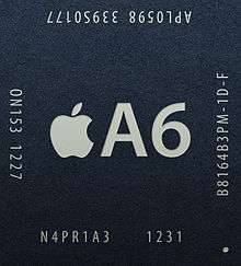 |
32 nm HKMG[52][91] | 96.71 mm2[52][91] | ARMv7s | 1.3 GHz[92] dual-core Swift[49] | L1i: 32 KB L1d: 32 KB L2: 1 MB[93] |
PowerVR SGX543MP3 (tri-core) @ 266 MHz (25.5 GFLOPS)[51] | 32-bit Dual-channel 533 MHz LPDDR2-1066[94] (8.528 GB/sec) | September 2012 | ||
| A6X | APL5598 |  |
32 nm HKMG[55] | 123 mm2[55] | ARMv7s | 1.4 GHz dual-core Swift[54] | L1i: 32 KB L1d: 32 KB L2: 1 MB |
PowerVR SGX554MP4 (quad-core) @ 266 MHz (68.1 GFLOPS)[54][95] | 32-bit Quad-channel 533 MHz LPDDR2-1066 (17.1 GB/sec)[96] | October 2012 | ||
| A7 | APL0698 |  |
28 nm HKMG[64] | 102 mm2[59] | ARMv8-A[60] | 1.3[57] GHz dual-core Cyclone[60] | L1i: 64 KB L1d: 64 KB L2: 1 MB L3: 4 MB[60] (Inclusive)[97] |
PowerVR G6430 (quad-core) @ 450 MHz (115.2 GFLOPS)[62][95] | 64-bit Single-channel 800 MHz LPDDR3-1600[68] (12.8 GB/sec)[98] | September 2013 | ||
| APL5698 |  |
28 nm HKMG[99] | 102 mm2[59][99] | 1.4[58] GHz dual-core Cyclone[60] | L1i: 64 KB L1d: 64 KB L2: 1 MB L3: 4 MB[58] (Inclusive)[97] |
PowerVR G6430 (quad-core) @ 450 MHz (115.2 GFLOPS)[95] | 64-bit Single-channel 800 MHz LPDDR3-1600[68] (12.8 GB/sec)[98] | October 2013 | ||||
| A8 | APL1011 | 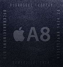 |
20 nm HKMG (TSMC)[68] | 89 mm2[100] | ~2 billion | ARMv8-A[67] | 1.1–1.5 GHz dual-core Typhoon[67][101] | L1i: 64 KB L1d: 64 KB L2: 1 MB L3: 4 MB[67] (Inclusive)[97] |
PowerVR GX6450 (quad-core)[102][103] iPhone 6+ | 64-bit Single-channel 800 MHz LPDDR3-1600[68] (12.8 GB/sec)[98] | September 2014 | |
| A8X | APL1012 |  |
20 nm HKMG (TSMC)[74][104] | 128 mm2[74] | ~3 billion | ARMv8-A | 1.5 GHz triple-core Typhoon[74][101] | L1i: 64 KB L1d: 64 KB L2: 2 MB L3: 4 MB[74] (Inclusive)[97] |
PowerVR GXA6850 (octa-core)[74][104] | 64-bit Dual-channel 800 MHz LPDDR3-1600[74] (25.6 GB/sec)[98] | October 2014 | |
| A9 | APL0898 |  |
14 nm FinFET (Samsung)[105] | 96 mm2[106] | >2 billion | ARMv8-A | 1.85 GHz dual-core Twister[107][108] | L1i: 64 KB L1d: 64 KB L2: 3 MB L3: 4 MB (Victim)[97][109] |
PowerVR GT7600 (hexa-core)[110] | 64-bit Single-channel 1600 MHz LPDDR4-3200[108][109] (25.6 GB/sec).[108] | September 2015 | |
| APL1022 | 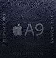 |
16 nm FinFET (TSMC)[106] | 104.5 mm2[106] | |||||||||
| A9X | APL1021 | 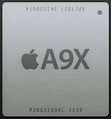 |
16 nm FinFET (TSMC)[111] | 147 mm2[111] | >3 billion | ARMv8-A | 2.16–2.26 GHz dual-core Twister[112][113] | L1i: 64 KB L1d: 64 KB L2: 3 MB L3: none[97][111] |
PowerVR 7XT Series (dodeca-core custom design)[111] | 64-bit Dual-channel 1600 MHz LPDDR4-3200 (51.2 GB/sec). | November 2015 | |
| A10 Fusion | APL1W24 | 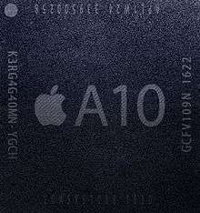 |
16 nm FinFET (TSMC)[114] | 125 mm2[114] | 3.3 billion | ARMv8-A | 2.34 GHz quad-core Hurricane (2+2 Fusion)[115] |
L1i: 64 KB L1d: 64 KB L2: 3 MB L3: 4 MB |
Hexa-core[116] | LPDDR4 | September 2016 |
S series
| Name | Model no. | Image | Semiconductor technology | Die size | CPU ISA | CPU | CPU cache | GPU | Memory technology | Introduced | Utilizing devices |
|---|---|---|---|---|---|---|---|---|---|---|---|
| S1 | APL0778[117] | 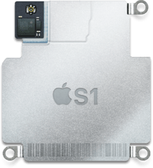 |
28 nm HKMG[118][119] | 32 mm2[118] | ARMv7k[119][120] | 520 MHz single-core Cortex-A7[119] | L1d: 32 KB[119] L2: 256 KB[119] |
PowerVR Series 5[119][121] | LPDDR3[122] | April 2015 | |
| S1P | APL**** |  |
ARMv8-A[123][124] | 780 MHz dual-core Typhoon | L1d: 64 KB L2: 1 MB |
TBA | LPDDR3 | September 2016 |
| ||
| S2 | APL**** |  |
ARMv8-A | 780 MHz dual-core Typhoon with GPS | L1d: 64 KB L2: 1 MB |
TBA | LPDDR3 | September 2016 |
|
T series
| Name | Model no. | Image | Semiconductor technology | Die size | CPU ISA | CPU | CPU cache | GPU | Memory technology | Introduced | Utilizing devices |
|---|---|---|---|---|---|---|---|---|---|---|---|
| T1 | APL1023[125] | No GPU | October 2016 |
W series
| Name | Model no. | Image | Semiconductor technology | Die size | CPU ISA | CPU | CPU cache | GPU | Memory technology | Introduced | Utilizing devices |
|---|---|---|---|---|---|---|---|---|---|---|---|
| W1 | APL**** | No GPU | September 2016 |
|
See also
- Apple motion coprocessors
- List of Historical Samsung Systems on a Chip
- ARM Cortex-A9 MPCore
- PowerVR SGX GPUs were also used in the iPhone 3GS and the third-generation iPod Touch
- PWRficient, a processor designed by P.A. Semi, a company Apple acquired to form an in-house custom chip design department
Similar platforms
- BCM2xxxx by Broadcom
- A31 by AllWinner
- Atom by Intel
- Exynos by Samsung
- i.MX by Freescale Semiconductor
- Jaguar and Puma by AMD
- MTxxxx by MediaTek
- NovaThor by ST-Ericsson
- OMAP by Texas Instruments
- RK3xxx by Rockchip
- Snapdragon by Qualcomm
- Tegra by Nvidia
References
- ↑ "The Most Important Apple Executive You've Never Heard Of". Bloomberg.com. Retrieved 2016-06-18.
- ↑ "iPhone 1st Generation Teardown". iFixit. June 29, 2007. Retrieved September 19, 2013.
- 1 2 3 4 5 6 7 8 9 10 11 Choi, Young (May 10, 2010). "Analysis gives first look inside Apple's A4 processor". EETimes. Archived from the original on September 14, 2013. Retrieved September 15, 2013.
- ↑ "iPod Touch 2nd Generation Teardown". iFixit. September 10, 2008. Retrieved September 19, 2013.
- 1 2 3 Lal Shimpi, Anand (June 10, 2009). "The iPhone 3GS Hardware Exposed & Analyzed". AnandTech. Retrieved September 13, 2013.
- ↑ Clark, Don (April 5, 2010). "Apple iPad Taps Familiar Component Suppliers - WSJ.com". Online.wsj.com. Retrieved April 15, 2010.
- ↑ "iPad - It's thin, light, powerful, and revolutionary". Apple. Archived from the original on July 6, 2010. Retrieved July 7, 2010.
- 1 2 "Apple Launches iPad" (Press release). Apple. January 27, 2010. Archived from the original on January 30, 2010. Retrieved January 28, 2010.
- ↑ "iPhone 4 design". Apple. July 6, 2010.
- ↑ Vance, Ashlee (February 21, 2010). "For Chip Makers, the Next Battle Is in Smartphones". New York Times. Archived from the original on February 25, 2010. Retrieved February 25, 2010.
- ↑ "iPad — Technical specifications". Apple. Retrieved October 16, 2016.
- ↑ Wiens, Kyle (April 5, 2010). "conclusion from both hard and software analysis it uses an ARM Cortex-A8 core". Ifixit.com. Archived from the original on April 18, 2010. Retrieved April 15, 2010.
- ↑ Melanson, Donald (February 23, 2010). "iPad confirmed to use PowerVR SGX graphics". Engadget.
- 1 2 3 4 "Chipworks Confirms Apple A4 iPad chip is fabbed by Samsung in their 45-nm process". Chipworks. April 15, 2010. Archived from the original on September 21, 2010.
- ↑ Stokes, Jon (April 28, 2010). "Apple purchase of Intrinsity confirmed". Ars Technica. Archived from the original on April 28, 2010. Retrieved April 28, 2010.
- ↑ Merritt, Rick. "Samsung, Intrinsity pump ARM to GHz rate". EETimes.com. Retrieved April 23, 2010.
- ↑ Keizer, Gregg (April 6, 2010). "Apple iPad smokes past the iPhone 3GS in speed". PC World. Archived from the original on April 20, 2010. Retrieved April 11, 2010.
- ↑ Boldt, Paul; Scansen, Don; Whibley, Tim (June 16, 2010). "Apple's A4 dissected, discussed...and tantalizing". EETimes.com. Retrieved July 7, 2010.
- ↑ "Microsoft PowerPoint - Apple A4 vs SEC S5PC110A01" (PDF). Archived (PDF) from the original on July 4, 2010. Retrieved July 7, 2010.
- ↑ "Apple iPad 2 GPU Performance Explored: PowerVR SGX543MP2 Benchmarked - AnandTech :: Your Source for Hardware Analysis and News". AnandTech. Archived from the original on March 18, 2011. Retrieved March 15, 2011.
- ↑ "Teardown of Apple's 4th-gen iPod touch finds 256MB of RAM". Appleinsider.com. September 8, 2010. Archived from the original on September 11, 2010. Retrieved September 10, 2010.
- ↑ "Apple TV 2nd Generation Teardown". iFixit. September 30, 2010. Archived from the original on January 2, 2011. Retrieved January 4, 2011.
- ↑ "Apple reveals iPhone 4 has 512MB RAM, doubling iPad - report". Appleinsider.com. June 17, 2010. Archived from the original on July 4, 2010. Retrieved July 7, 2010.
- ↑ "A Peek Inside Apple's A4 Processor". iFixit. April 5, 2010.
- ↑ Greenberg, Marc (April 9, 2010). "Apple iPad: no LPDDR2?". Denali.
- ↑ Merritt, Rick (April 9, 2010). "iPad equipped to deliver richer graphics". EE Times Asia. Retrieved April 14, 2010.
- ↑ "Updated: Samsung fabs Apple A5 processor". EETimes.com. March 12, 2011. Archived from the original on May 9, 2013. Retrieved March 15, 2011.
- ↑ "Apple Announces iPad 2 with New Design, Faster A5 Processor".
- ↑ "Apple iPad 2 feature page". Apple.com. Archived from the original on March 16, 2011. Retrieved March 15, 2011.
- 1 2 "Apple iPad 2 Preview - AnandTech :: Your Source for Hardware Analysis and News". AnandTech. Retrieved March 15, 2011.
- ↑ "iPad 2 - Technical Specifications". Apple. Retrieved October 16, 2016.
- ↑ "Inside Apple's iPad 2 A5: fast LPDDR2 RAM, costs 66% more than Tegra 2". AppleInsider. Retrieved March 15, 2011.
- 1 2 3 "A First Look at Apple's A5 Processor". Chipworks. March 12, 2011. Retrieved September 15, 2013.
- 1 2 3 "Update – 32-nm Apple A5 in the Apple TV 3 – and an iPad 2!". Chipworks. April 11, 2012. Retrieved September 15, 2013.
- ↑ Single-core A5 CPU in new 1080p Apple TV doubles RAM to 512MB
- ↑ "Update – 32-nm Apple A5 in the Apple TV 3 – and an iPad 2!". Chipworks. April 11, 2012. Retrieved April 12, 2012.
- ↑ "The iPad 2,4 Review: 32nm Brings Better Battery Life". AnandTech. Retrieved November 1, 2012.
- ↑ A5 Chip in Tweaked Apple TV Still Manufactured by Samsung at 32nm - MacRumors.com
- ↑ Tweaked Apple TV Contains Die-Shrunk A5 Chip, Not A5X - MacRumors.com
- 1 2 3 "Apple's TV surprise – a new A5 chip!". Chipworks. March 12, 2013. Retrieved September 15, 2013.
- ↑ "Apple Launches New iPad". Apple. March 7, 2012. Retrieved September 17, 2013.
- 1 2 3 "The Apple A5X versus the A5 and A4 – Big Is Beautiful". Chipworks. March 19, 2012. Retrieved September 15, 2013.
- ↑ "Apple A5X Die Size Measured: 162.94mm^2, Samsung 45nm LP Confirmed". AnandTech. Retrieved November 1, 2012.
- ↑ "The Frequency of Apple A5X in the New iPad Confirmed: Still Running at 1GHz". AnandTech. Retrieved November 1, 2012.
- ↑ "iFixit teardown of the 3rd generation iPad.". iFixit.
- ↑ Apple Introduces iPhone 5, Apple.com, September 12, 2012, retrieved September 20, 2012
- ↑ Apple: A6 chip in iPhone 5 has 2x CPU power, 2x graphics performance, yet consumes less energy
- ↑ Apple's A6 CPU actually clocked at around 1.3 GHz, per new Geekbench report, Engadget, September 26, 2012, retrieved September 26, 2012
- 1 2 3 Lal Shimpi, Anand (September 15, 2012). "The iPhone 5's A6 SoC: Not A15 or A9, a Custom Apple Core Instead". AnandTech. Retrieved September 15, 2012.
- ↑ Lal Shimpi, Anand; Klug, Brian; Gowri, Vivek (October 16, 2012). "The iPhone 5 Review - Decoding Swift". AnandTech. Retrieved October 17, 2012.
- 1 2 "Apple A6 Die Revealed: 3-core GPU, <100mm^2". AnandTech. September 21, 2012. Retrieved September 22, 2012.
- 1 2 3 "Apple iPhone 5 – the A6 Application Processor". Chipworks. September 21, 2012. Archived from the original on September 15, 2013. Retrieved September 15, 2013.
- ↑ "Apple Introduces iPad mini". Apple. October 23, 2012. Retrieved September 16, 2013.
- 1 2 3 4 Lal Shimpi, Anand (November 2, 2012). "iPad 4 GPU Performance Analyzed: PowerVR SGX 554MP4 Under the Hood". AnandTech. Retrieved September 16, 2013.
- 1 2 3 4 "Inside the Apple iPad 4 – A6X a very new beast!". Chipworks. November 1, 2012. Retrieved September 15, 2013.
- ↑ "Apple Announces iPhone 5s—The Most Forward-Thinking Smartphone in the World". Apple. September 10, 2013. Retrieved September 13, 2013.
- 1 2 3 4 Lal Shimpi, Anand (September 17, 2013). "The iPhone 5s Review: A7 SoC Explained". AnandTech. Retrieved September 18, 2013.
- 1 2 3 Lai Shimpi, Anand (October 29, 2013). "The iPad Air Review: iPhone to iPad: CPU Changes". AnandTech. Retrieved October 30, 2013.
- 1 2 3 4 Lal Shimpi, Anand (September 17, 2013). "The iPhone 5s Review: The Move to 64-bit". AnandTech. Retrieved September 18, 2013.
- 1 2 3 4 5 6 Lal Shimpi, Anand (September 17, 2013). "The iPhone 5s Review: After Swift Comes Cyclone". AnandTech. Retrieved September 18, 2013.
- ↑ "[LLVMdev] A7 processor support?". LLVM Developers Mailing List. September 10, 2013. Retrieved September 11, 2013.
- 1 2 Lal Shimpi, Anand (September 17, 2013). "The iPhone 5s Review: GPU Architecture". AnandTech. Retrieved September 18, 2013.
- ↑ Cunningham, Andrew (September 10, 2013). "Apple unveils 64-bit iPhone 5S with fingerprint scanner, $199 for 16GB". Ars Technica. Retrieved September 12, 2013.
- 1 2 Tanner, Jason; Morrison, Jim; James, Dick; Fontaine, Ray; Gamache, Phil (September 20, 2013). "Inside the iPhone 5s". Chipworks. Archived from the original on August 3, 2014. Retrieved September 20, 2013.
- ↑ "Apple Announces iPhone 6 & iPhone 6 Plus—The Biggest Advancements in iPhone History" (Press release). Apple. September 9, 2014. Retrieved September 9, 2014.
- ↑ Savov, Vlad (September 9, 2014). "iPhone 6 and iPhone 6 Plus have a new faster A8 processor". The Verge. Vox Media. Retrieved September 9, 2014.
- 1 2 3 4 5 "The iPhone 6 Review: A8's CPU: What Comes After Cyclone?". AnandTech. September 30, 2014. Retrieved September 30, 2014.
- 1 2 3 4 5 6 "The iPhone 6 Review: A8: Apple's First 20nm SoC". AnandTech. September 30, 2014. Retrieved September 30, 2014.
- ↑ Smith, Ryan (September 9, 2014). "Apple Announces A8 SoC". AnandTech. Retrieved September 9, 2014.
- ↑ "Inside the iPhone 6 and iPhone 6 Plus". Chipworks. September 19, 2014. Retrieved September 20, 2014.
- ↑ Anthony, Sebastian. "Apple's A8 SoC analyzed: The iPhone 6 chip is a 2-billion-transistor 20nm monster". www.extremetech.com. ExtremeTech. Retrieved September 10, 2014.
- 1 2 "Apple Introduces iPad Air 2—The Thinnest, Most Powerful iPad Ever" (Press release). Apple. October 16, 2014. Retrieved October 16, 2014.
- ↑ "iPad Air 2 - Performance". Apple. October 16, 2014. Retrieved October 16, 2014.
- 1 2 3 4 5 6 7 8 "Apple A8X's GPU - GXA6850, Even Better Than I Thought". Anandtech. November 11, 2014. Retrieved November 12, 2014.
- 1 2 "Apple Introduces iPhone 6s & iPhone 6s Plus" (Press release). Apple. September 9, 2015. Retrieved September 9, 2015.
- ↑ "Apple Introduces iPad Pro Featuring Epic 12.9-inch Retina Display" (Press release). Apple. September 9, 2015. Retrieved September 9, 2015.
- ↑ "Apple's new iPad Pro is an expansive 12.9 inches, available in November". Ars Technica. Retrieved 9 September 2015.
- ↑ "Apple Introduces iPhone 7 & iPhone 7 Plus —The Best, Most Advanced iPhone Ever" (Press release). Apple. September 7, 2016. Retrieved September 16, 2016.
- ↑ http://www.technobuffalo.com/2014/09/09/apple-watch-uses-a-new-s1-chip-heart-rate-monitor/
- ↑ Apple Creates Its First Wireless Chip For New Wireless Headphones, AirPods
- ↑ Apple Announces New Line of Beats Headphones With W1 Wireless Chip
- ↑ Apple’s AirPods do use Bluetooth and they don’t require an iPhone 7
- ↑ AirPods - Apple
- ↑ Smith, Ryan (27 October 2016). "Apple Announces 4th Generation MacBook Pro Family: Thinner, Lighter, with Thunderbolt 3 & "Touchbar"". Anandtech. Retrieved 27 October 2016.
- ↑ Cunningham, Andrew (28 October 2016). "15 hours with the 13" MacBook Pro, and how Apple's T1 bridges ARM and Intel". Ars Technica. Retrieved 28 October 2016.
- ↑ Lal Shimpi, Anand; Klug, Brian (October 31, 2011). "Apple iPhone 4S: Thoroughly Reviewed - The Memory Interface". AnandTech. Retrieved September 15, 2013.
- ↑ iPod Nano 4th Generation Teardown
- ↑ Wiens, Kyle (2010-04-05). "conclusion from both hard and software analysis it uses an ARM Cortex-A8 core". Ifixit.com. Archived from the original on 18 April 2010. Retrieved 2010-04-15.
- 1 2 3 4 Lal Shimpi, Anand (Sep 2012). "The iPhone 5 Performance Preview". AnandTech. Retrieved October 24, 2012.
- ↑ "The Apple iPad Review (2012)". AnandTech. Retrieved November 1, 2012.
- 1 2 "Apple A6 Teardown". IFixit. September 25, 2012.
- ↑ "The iPhone 5 Performance Preview". AnandTech. Retrieved November 1, 2012.
- ↑ iPhone 5 Benchmarks Appear in Geekbench Showing a Dual Core, 1 GHz A6 CPU
- ↑ Shimpi, Anand Lal; Klug, Brian (September 15, 2012). "iPhone 5 Memory Size and Speed Revealed: 1 GB LPDDR2-1066". AnandTech. Retrieved September 16, 2012.
- 1 2 3 Lai Shimpi, Anand (October 29, 2013). "The iPad Air Review: GPU Performance". AnandTech. Retrieved October 30, 2013.
- ↑ "iPad 4 (Late 2012) Review". AnandTech. Retrieved July 10, 2013.
- 1 2 3 4 5 6 "Correcting Apple's A9 SoC L3 Cache Size: A 4MB Victim Cache". AnandTech. November 30, 2015. Retrieved December 1, 2015.
- 1 2 3 4 "The Apple iPad Air 2 Review". AnandTech. Retrieved November 12, 2014.
- 1 2 "Inside the iPad Air". Chipworks. November 1, 2013.
- ↑ "Apple's A8 SoC analyzed". ExtremeTech. September 10, 2014.
- 1 2 Chester, Brandon (July 15, 2015). "Apple Refreshes The iPod Touch With A8 SoC And New Cameras". Retrieved September 11, 2015.
- ↑ "Chipworks Disassembles Apple's A8 SoC: GX6450, 4MB L3 Cache & More". AnandTech. September 23, 2014.
- ↑ "Imagination PowerVR GX6450". NOTEBOOKCHECK. September 23, 2014.
- 1 2 "Imagination PowerVR GXA6850 - NotebookCheck.net Tech". NotebookCheck.net. November 26, 2014. Retrieved November 26, 2014.
- ↑ Ho, Joshua (September 9, 2015). "Apple Announces the iPhone 6s and iPhone 6s Plus". Retrieved September 10, 2015.
- 1 2 3 "Apple's A9 SoC Is Dual Sourced From Samsung & TSMC". Anandtech. September 28, 2015. Retrieved September 29, 2015.
- ↑ "iPhone 6s customer receives her device early, benchmarks show a marked increase in power". iDownloadBlog. September 21, 2015. Retrieved September 25, 2015.
- 1 2 3 "A9's CPU: Twister - The Apple iPhone 6s and iPhone 6s Plus Review". AnandTech. November 2, 2015. Retrieved November 4, 2015.
- 1 2 "Inside the iPhone 6s". Chipworks. September 25, 2015. Retrieved September 26, 2015.
- ↑ "A9's GPU: Imagination PowerVR GT7600 - The Apple iPhone 6s and iPhone 6s Plus Review". AnandTech. November 2, 2015. Retrieved November 4, 2015.
- 1 2 3 4 "More on Apple's A9X SoC: 147mm2@TSMC, 12 GPU Cores, No L3 Cache". AnandTech. November 30, 2015. Retrieved December 1, 2015.
- ↑ "The A9X SoC & More To Come - The iPad Pro Preview: Taking Notes With iPad Pro". AnandTech. November 11, 2015. Retrieved November 11, 2015.
- ↑ "iPad Pro review: Mac-like speed with all the virtues and restrictions of iOS". AnandTech. November 11, 2015. Retrieved November 11, 2015.
- 1 2 Apple iPhone 7 Teardown
- ↑ macOS 10.12 API Diffs - Kernel Changes for Objective-C
- ↑ Apple Announces iPhone 7 & iPhone 7 Plus: A10 Fusion SoC, New Camera, Wide Color Gamut, Preorders Start Sept. 9th
- ↑ "Teardown shows Apple Watch S1 chip has custom CPU, 512MB RAM, 8GB storage". AppleInsider. Retrieved 30 April 2015.
- 1 2 Jim Morrison and Daniel Yang (April 24, 2015). "Inside the Apple Watch: Technical Teardown". Chipworks.
- 1 2 3 4 5 6 Ho, Joshua; Chester, Brandon (July 20, 2015). "The Apple Watch Review: Apple S1 Analysis". AnandTech. Retrieved July 20, 2015.
- ↑ Hopper happily opens Apple Watch binaries ('armv7k') to disassemble, says they're 'armv7m'. -- Steve Troughton-Smith
- ↑ "Apple Watch runs 'most' of iOS 8.2, may use A5-equivalent processor". AppleInsider. Retrieved 25 April 2015.
- ↑ Ho, Joshua; Chester, Brandon (July 20, 2015). "The Apple Watch Review". AnandTech. Retrieved July 20, 2015.
- ↑ We Just Took Apart the Apple Watch Series 1—Here’s What We Found Out
- ↑ Apple Introduces Apple Watch Series 2, The Ultimate Device For A Healthy Life
- ↑ "MacBook Pro 13" Touch Bar Teardown". iFixit. Retrieved 17 November 2016.
| Founders | |||||||||||
|---|---|---|---|---|---|---|---|---|---|---|---|
| Board of directors |
| ||||||||||
| Executives |
| ||||||||||
| Services |
| ||||||||||
| Products |
| ||||||||||
| Companies |
| ||||||||||
| Related | |||||||||||
| |||||||||||