Adhesive bonding
Adhesive bonding (also referred to as gluing or glue bonding) describes a water bonding technique with applying an intermediate layer to connect substrates of different materials. These produced connections can be soluble or insoluble.[1] The commercially available adhesive can be organic or inorganic and is deposited on one or both substrate surfaces. Adhesives, especially the well-established SU-8, and benzocyclobutene (BCB), are specialized for MEMS or electronic component production.[2]
The procedure enables bonding temperatures from 1000 °C down to room temperature.[1] The most important process parameters for achieving a high bonding strength are:[3]
- adhesive material
- coating thickness
- bonding temperature
- processing time
- chamber pressure
- tool pressure
Adhesive bonding has the advantage of relatively low bonding temperature as well as the absence of electric voltage and current. Based on the fact that the wafers are not in direct contact, this procedure enables the use of different substrates, e.g. silicon, glass, metals and other semiconductor materials. A drawback is that small structures become wider during patterning which hampers the production of an accurate intermediate layer with tight dimension control.[3] Further, the possibility of corrosion due to out-gassed products, thermal instability and penetration of moisture limits the reliability of the bonding process.[4] Another disadvantage is the missing possibility of hermetically sealed encapsulation due to higher permeability of gas and water molecules while using organic adhesives.[5]
Overview
The adhesive bonding with organic materials, i.e. BCB or SU-8, has simple process properties and the ability to form high aspect ratio micro structures. The bonding procedure is based on polymerization reaction of organic molecules to form long polymer chains during annealing. This cross-link reaction forms BCB and SU-8 to a solid polymer layer.[3]
The intermediate layer is applied by spin-on, spray-on, screen-printing, embossing, dispensing or block printing on one or two substrate surfaces. The adhesive layer thickness depends on the viscosity, rotational speed and the applied tool pressure. The procedural steps of adhesive bonding are divided into the following:[1]
- Cleaning and pre-treatment of substrates surfaces
- Application of adhesive, solvent or other intermediate layers
- Contacting substrates
- Hardening intermediate layer
The most established adhesives are polymers that enable connections of different materials at temperatures ≤ 200 °C.[5] Due to these low process temperature metal electrodes, electronics and various micro-structures can be integrated on the wafer. The structuring of polymers as well as the realization of cavities over movable elements are possible using photo-lithography or dry etching.[5]
The hardening conditions depend on the used materials. Hardening of the adhesives are possible:[1]
- at room temperature
- through heating cycles
- using UV light
- by applying pressure
SU-8
Overview
SU-8 is a 3 component UV-sensitive negative photo-resist based on epoxy resin, gamma butyrolactone and triaryl sulfonium salt. The SU-8 polymerizes at approximately 100 °C and is temperature-stable up to 150 °C. This polymer adhesive is CMOS and bio-compatible and has excellent electrical, mechanical and fluidic properties. It also has a high cross-linking density, high chemical resistance and high thermal stability. The viscosity depends on the mixture with the solvent for different layer thicknesses (1.5 to 500 µm). Using multilayer coating a layer thickness up to 1 mm is reachable. The lithographic structuring is based on a photoinitiator triaylium-sulfonium that releases lewis acid during UV radiation. This acid works as catalyst for the polymerization. The connection of the molecules is activated over different annealing steps, so called post exposure bake (peb).[5] Using SU-8 can achieve a high bonding yield. In addition, the substrate flatness, clean room conditions and the wettability of the surface are important factors to achieve good bond results.[6]
Procedural steps
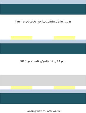
The standard process (compare to figure "Schematic bonding process") consists of applying SU-8 on the top wafer by spin-on or spray-on of thin layers (3 to 100 µm).
Subsequently, the structuring of the photo-resist using direct UV light exposure is applied but can also be achieved through deep reactive-ion-etching (DRIE). During coating and structuring of the SU-8 the tempering steps before and after exposure have to be considered. Based on thermal layer stress the risk of crack formation exists. While coating the photoresist the formation of voids due to the layer thickness inhomogeneity has to be avoided. The adhesive layer thickness should be larger than the flatness imperfection of the wafer to establish good contact.[3] The procedural steps based on a typical example are:
- Cleaning Top wafer
- Thermal oxidation
- Dehydration
- Spin coating the SU-8
- Softbake
- 120 s at 65 °C
- 300 s to 95 °C
- Cooling down
- Exposure with 165 to 200 mJ⁄cm3
- Post-exposure-bake
- 2 to 120 min at 50 to 120 °C
- to room temperature
- relaxation time
- development
- rinsing and dry spinning
- hard bake at 50 to 150 °C for 5 to 120 min

For non-planar wafer surfaces or free standing structures, spin-coating is not a very successful SU-8 deposition method. As a result, spray-on is mainly used on structured wafers.[6] The bonding takes place at the polymerization temperature of SU-8 at approximately 100 °C.
The soft-bake allows that high residual solvent content minimizes intrinsic stress and improves cross-linking. The SU-8 layer is patterned using soft contact exposure followed by post-exposure bake. The non-exposed SU-8 is removed by immersing in, e.g. propylene glycol methyl ether acetate (PGMEA).[7]
Ensuring void-free bonding a homogeneous layer thickness of the SU-8 over the wafer surface is important (compare to cross section photo).[5]
To ensure good contact of the wafer pair a constant pressure between 2.5 and 4.5 bar during bonding is applied.[3]
The frames should be kept above the non-flatness value of the wafer, based on the fact that defects usually are caused by the curvature of the wafer.[3] A shear strength of the bonded wafer pair of about 18 to 25 MPa is achievable.[6]
Examples
Adhesive bonding using SU-8 is applicable to zero-level packaging technology for low cost MEMS packaging. Metallic feed-throughs can be used for electrically connections to packed elements through the adhesive layer.[7] Also biomedical and micro fluidic devices are fabricated based on SU-8 adhesive layer as well as micro fluidic channels, movable micro-mechanical components, optical waveguides and UV-LIGA components.[8]
Benzocyclobutene (BCB)
Overview

Benzocyclobutene (BCB) is a hydrocarbon that is widely used in electronics.[10] BCB exists in a dry etch and a photosensitive version, each requiring different procedural steps for structuring (compare BCB process flow).[11]
It does release only small amounts of by-products during curing which enables a void-free bond. This polymer ensures very strong bonds and excellent chemical resistance to numerous acids, alkalines and solvents. The BCB is over 90% transparent to visible light that enables the use for optical MEMS applications.[10]
Compared to other polymers the BCB has a low dielectric constant and dielectric loss.[12] The polymerization of BCB is taking place at a temperature around 250 to 300 °C and it is stable up to 350 °C. Using BCB does not ensure a sufficient hermeticity of sealed cavities for MEMS.[13]
Procedural steps
The procedural steps for dry etch BCB are:
- Cleaning
- Supplying the adhesion promoter
- Drying of the primer
- BCB deposition
- Photosensitive BCB
- Exposure and development
- Dry etch BCB
- Pre-bake/soft-cure
- Patterning of the BCB layer by lithography and dry-etching
- Bonding at specific temperature, ambient pressure for specific amount of time
- Post-bake/hard-cure to form solid BCB monomer layer
The wafers can be cleaned using H2O2 + H2SO4 or oxygen plasma. The cleaned wafers are rinsed with DI water and dried at elevated temperature, e.g. 100 to 200 °C for 120 min.[11]
The adhesion promoter with a specific thickness is deposited, i.e. spin-coated or contact printed on the wafer to improve the bonding strength. Spray coating is preferable when the adhesive is deposited on free standing structures.[13]

Subsequently the BCB layer is spin or spray coated, usually 1 to 50 µm thick, to the same wafer. To prevent that the patterned layer has a lower bond strength than the unpatterned layer, due to the cross-linking of the polymer, a soft-curing step is applied before bonding.[14] The pre-curing of the BCB takes place for several minutes on the hot plate at a specific temperature ≤ 300 °C. The soft cure prevents bubble formation and unbonded areas[15] as well as the distortion of the adhesive layer during compression to improve the alignment accuracy.[16] The degree of polymerization should not be over 50%, so it is robust enough to be patterned and still sufficiently adhesive to be bonded.[14]
If the BCB is hard-baked (far over 50%), it loses its adhesives properties and results in an increased amount of void formation. But also if the soft-curing is above 210 °C the adhesive cures too much, so that the material is not soft and sticky enough to achieve a high bonding strength.[9]
The substrates with the intermediate layer are pressed together with subsequent curing results in a bond.[4] The post-bake process is applied at 180 to 320 °C for 30 to 240 min usually in a specific atmosphere or vacuum in the bond chamber. This is necessary to hard-cure the BCB. The vacuum prevents air trapped in the bond interface and pumps out the gases of the out-gassing residual solvents during annealing. The temperature and the curing time are variable, so with a higher temperature curing time can be reduced based on a quicker cross-linking.[10] The final bonding layer thickness depends on the thickness of the cured BCB, the spinning speed and the shrink rate.[9]
Examples
Adhesive bonding using a BCB intermediate layer is a possible method for packaging and sealing of MEMS devices, also structured Si wafers. Its use is specified for applications that does not require hermetic sealing, i.e. MOEMS mirror arrays, RF MEMS switches and tunable capacitors. BCB bonding is used in the fabrication of channels for fluidic devices, for transfer protruding surface structures as well as for CMOS controller wafers and integrated SMA microactuators.
Technical Specifications
| Materials |
Substrate:
Intermediate layer:
|
| Temperature |
|
| Advantages |
|
| Drawbacks |
|
| Researches |
|
References
- 1 2 3 4 Wiemer, M.; Frömel, J.; Gessner, T. (2003). "Trends der Technologieentwicklung im Bereich Waferbonden". In W. Dötzel. 6. Chemnitzer Fachtagung Mikromechanik & Mikroelektronik. 6. pp. 178–188.
- ↑ Gessner, T.; Otto, T.; Wiemer, M.; Frömel, J. (2005). "Wafer bonding in micro mechanics and microelectronics - an overview". The World of Electronic Packaging and System Integration. pp. 307–313.
- 1 2 3 4 5 6 7 8 9 Wiemer, M.; Jia, C.; Töpper, M.; Hauck, K. (2006). "Wafer Bonding with BCB and SU-8 for MEMS Packaging". Electronics Systemintegration Technology Conference. 1st Electronics Systemintegration Technology Conference, 2006. 1. pp. 1401–1405. doi:10.1109/ESTC.2006.280194. ISBN 1-4244-0552-1.
- 1 2 Wolffenbuttel, R. F. (1997). "Low-temperature intermediate Au-Si wafer bonding; eutectic or silicide bond". Sensors and Actuators A: Physical. 62 (1-3). pp. 680–686. doi:10.1016/S0924-4247(97)01550-1.
- 1 2 3 4 5 Reuter, D.; Frömel, J.; Schwenzer, G.; Bertz, A.; Gessner, T. (October 2003). "Selektives Niedertemperaturbonden mit SU-8 für Wafer-Level-Verkappung von mikromechanischen Strukturen". In W. Dötzel. 6. Chemnitzer Fachtagung Mikromechanik & Mikroelektronik. 6. Technische Universität Chemnitz. pp. 90–94.
- 1 2 3 Yu, L.; Tay, F. E. H.; Xu, G.; Chen, B.; Avram, M.; Iliescu, C. (2006). "Adhesive bonding with SU-8 at wafer level for microfluidic devices". Journal of Physics: Conference Series. 34 (1). p. 776.
- 1 2 Murillo, G.; Davis, Z. J.; Keller, S.; Abadal, G.; Agusti, J.; Cagliani, A.; Noeth, N.; Boisen, A.; Barniol, N. (2010). "Novel SU-8 based vacuum wafer-level packaging for MEMS devices". Microelectronic Engineering. 87 (5-8). pp. 1173–1176. doi:10.1016/j.mee.2009.12.048.
- ↑ Patel, J. N.; Kaminska, B.; Gray, B. L.; Gates, B. D. (2008). "PDMS as a sacrificial substrate for SU-8-based biomedical and microfluidic applications". Journal of Micromechanics and Microengineering. 18 (9). p. 095028.
- 1 2 3 Oberhammer, J.; Niklaus, F.; Stemme, G. (2003). "Selective wafer-level adhesive bonding with benzocyclobutene for fabrication of cavities". Sensors and Actuators A: Physical. 105 (3). pp. 297–304. doi:10.1016/S0924-4247(03)00202-4.
- 1 2 3 Niklaus, F.; Andersson, H.; Enoksson, P.; Stemme, G. (2001). "Low temperature full wafer adhesive bonding of structured wafers". Sensors and Actuators A: Physical. 92 (1-3). pp. 235–241. doi:10.1016/S0924-4247(01)00568-4.
- 1 2 Christiaens, I.; Roelkens, G.; De Mesel, K.; van Thourhout, D.; Baets, R. (2005). "Thin-film devices fabricated with benzocyclobutene adhesive wafer bonding". Journal of Lightwave Technology. 23 (2). pp. 517–523. doi:10.1109/JLT.2004.841783.
- ↑ Töpper, M.; Lopper, C.; Zoschke, K.; Scherpinski, K.; Fritzsch, T.; Dietrich, L.; Lutz, M.; Ehrmann, O.; Reichl, H. BCB - A Thin Film Polymer for Advanced Wafer Level Packaging and MEMS Applications (Report). Fraunhofer IZM and TU Berlin. pp. 292–298.
- 1 2 Oberhammer, J.; Niklaus, F.; Stemme, G. (2004). "Sealing of adhesive bonded devices on wafer level". Sensors and Actuators A: Physical. 110 (1-3). pp. 407–412. doi:10.1016/j.sna.2003.06.003.
- 1 2 Oberhammer, J.; Stemme, G. (2004). "Contact printing for improved bond-strength of patterned adhesive full-wafer bonded 0-level packages". 17th IEEE International Conference on Micro Electro Mechanical Systems (MEMS). pp. 713–716. doi:10.1109/MEMS.2004.1290684.
- ↑ Niklaus, F.; Enoksson, P.; Kalvesten, E.; Stemme, G. (2000). "Void-free full wafer adhesive bonding". The 13th Annual International Conference on Micro Electro Mechanical Systems (MEMS). pp. 247–252. doi:10.1109/MEMSYS.2000.838524.
- ↑ Farrens, S. (2008). "Wafer-Bonding Technologies and Strategies for 3D ICs". In Tan, C. S.; Gutmann, R. J.; Reif, L. R. Wafer Level 3-D ICs Process Technology. Integrated Circuits and Systems. Springer US. pp. 49–85. doi:10.1007/978-0-387-76534-1.